반도체디스플레이기술학회지 제14권 제1호(2015년 3월)
Journal of the Semiconductor & Display Technology, Vol. 14, No. 1. March 2015.
27
대향 타겟 스퍼터링법으로 제작한 SiC SBD의 전기적 특성
이진선 · 강태영* · 김경환
†
†
가천대학교 전기공학과*파워큐브세미㈜
Electrical Characteristics of the SiC SBD Prepared by using the Facing Targets Sputtering Method
Jinseon Lee, Tai Young Kang* and Kyung Hwan Kim
†
†
Department of Electrical engineering, Gachon Universitym*Powercubesemi Incorporation
Abstract
SiC based Schottky barrier diodes were prepared by using the facing targets sputtering method. In this research, 4H- SiC polytypes of SiC were adopted and Molybdenum, Titanium was employed as the Schottky metal of the metal- semiconductor contacts. Both structures showed the rectifying nature in their forward and reverse J-V characteristic curve and the ideality factors calculated from these plots that were close to unity were represented the nearly ideal behavior.
Difference of Schottky barrier height between prepared devices was also corresponding with the electrical characteristics of themselves. Therefore the suitability of the facing targets sputtering method for fabrication of Schottky diodes could be suggested from these results.
Key Words : Silicon carbide, Facing Targets sputtering, Schottky barrier diode, Schottky diode parameter
1. 서 론
탄화규소(Silicon Carbide: SiC)는 우수한 전기적, 열 적 특성에 의해 소자 성능 개선의 한계에 당면하고 있 는 것으로 평가되고 있는 Si를 대체할 수 있는 반도체 재료로써, 전력 반도체 분야에서 광범위한 연구가 진행 되고 있다[1]. SiC는 높은 밴드갭, 열 전도도에 의해 높 은 온도에서도 소자의 안정적인 동작을 및 열 소산 형 태의 에너지 손실 저감이 가능하다[2]. 특히 높은 절연 파괴 강도는 고전압 소자의 제작에 매우 적합한 특성 이며, Si의 물성적 한계에 의해 낮은 전압 범위로 제한 되는 쇼트키 다이오드(Schottky barrier diode: SBD)와 같은 같은 단극성 소자의 동작 범위를 큰 폭으로 확장 시킬 수 있다[3]. SBD의 정류 특성은 금속-반도체 간 의 접합에서 형성되는 쇼트키 장벽(Schottky Barrier)에
의한 비 선형적 전압-전류 특성에 기인하며 이러한 소 자의 동작은 열전자방출이론을 기반으로 하는 쇼트키 다이오드 방정식으로 설명될 수 있다[4,5]
(1)
수식에서 A**, q, k, T는 각각 열전자방출상수, 전자 의 전하량, 볼츠만 상수, 절대온도를 의미하는 상수항이 다. SBD의 전기적 특성은 쇼트키 장벽의 높이(Schottky barrier height: SBH), 소자의 직렬저항, 이상계수에 의해 결정되며 특히 SBH는 소자의 정류특성을 나타낼 수 있 는 지표라 할 수 있다. SBH(φB)는 Schottky-Mött theory 에 의해 반도체의 전자 친화도(ΧS)와 금속의 일함수(φM) 의 차이에 의해 예견될 수 있으며, 접합을 형성하는 금 속과 반도체 재료의 종류에 따라 다른 값을 보인다.
J A**T
2
exp qϕB
---kT⎝– ⎠
⎛ ⎞ exp qV
nkT---
⎝ ⎠
⎛ ⎞ 1–
=
Js exp qV nkT---
⎝ ⎠
⎛ ⎞ 1–
=
†
E-mail : [email protected]28 이진선 · 강태영 · 김경환
반도체디스플레이기술학회지 제14권 제1호, 2015 (2)
본 연구에서는 대향 타겟 스퍼터링법(the Facing Targets Sputtering: FTS)을 통해 4H-SiC wafer 위에 금 속 박막을 증착하여 SBD를 제작하고, 그 전기적 특성 을 평가하였으며 이상적인 소자 특성과 비교하였다.
2. 실험과정
2.1. 대향 타겟 스퍼터링
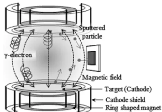
Fig. 1과 같이 대향 타겟 스퍼터링 시스템은 한 쌍의 서로 마주한 타겟과 이들의 중심에 수직한 곳에 위치한 기판으로 구성되어 있다.
이 구조에서 플라즈마를 발생, 유지시키는 하전입자들 은 수직자계에 의해 두 타겟 사이를 나선형으로 왕복하 며 방전기체의 이온화를 증가시켜 플라즈마의 밀도를 향 상시키며, 이는 스퍼터링 효율 개선효과를 수반한다. 플 라즈마 영역에서 이격된 기판의 위치 또한 고 에너지 입 자에 의한 기판 및 박막의 손상을 경감시킬 수 있어 증 착된 박막의 품위 향상에 기여할 수 있다[6,7].
2.2. 소자 제작 및 전기적 특성 평가
본 연구에서는 캐리어 농도 및 두께가 5 × 10
15
cm−3
, 11.5 μm인 drift layer를 포함하는 4H-SiC wafer를 기판 으로 사용하였으며 아세톤, 에탄올, 증류수의 순서로 초음파 세척 후 금속 박막을 증착하였다. 4H-SiC와 접 합을 형성하는 쇼트키 금속은 Mo와 Ti를 사용하였으 며 각각의 금속에 대한 증착 조건은 Table 1과 같다.제작된 소자의 전기적 특성을 평가하기 위해 High- Voltage Sourcemeter (Model 2410, Keithley Instruments Inc.) 및 I-V curve tracing software(24XX Basic Soft- ware, I.V Solution)를 사용하여 J-V 특성곡선을 측정하 고, 그로부터 소자 특성계수를 산출하였다.
3. 결과 및 고찰
Fig. 2는 대향 타겟 스퍼터링법을 통해 제작된 Mo/SiC 및 Ti/SiC SBD의 J-V 특성곡선이다. 특성곡선에서 나타 난 바와 같이 두 구조는 모두 정류 특성을 나타내었으며, 금속 물질의 차이에 의해 상이한 전기적 특성을 보였다.
이러한 차이에 의해 보다 정량적인 분석을 위해 Cheung
& Cheung method 및 Norde method를 사용하여 각 구 조의 소자 특성계수를 산출하였다. Cheung & Cheung method는 다음 두 수식에 의한 선형 그래프로부터 소 자 특성계수를 계산하는 방법이며, Fig. 3에 각각의 그 ϕ
B
=ϕM
–XS
Fig. 1. Schematics of the facing targets sputtering system.
Table 1. Sputtering conditions of the Schottky metal layers for SBDs
Deposition parameters
Sputtering condtions Mo/SiC Ti/SiC Targets Mo, 4N purity Ti, 4N purity Base pressure under 1×10
−6
torr Working pressure 1×10⁻³
torrGas ambient Ar, 4N puritiy, 10 sccm Input current 0.1 A Layer thickness 1000 Å
Fig. 2. Forward and reverse J-V characteristic curves of the Schottky diodes.
Fig. 3. Plots of the Cheung & Cheung method for the Schottky diodes.
대향 타겟 스퍼터링법으로 제작한 SiC SBD의 전기적 특성 29
Journal of KSDT Vol. 14, No. 1, 2015 래프를 나타내었다[8].
(3)
(4)
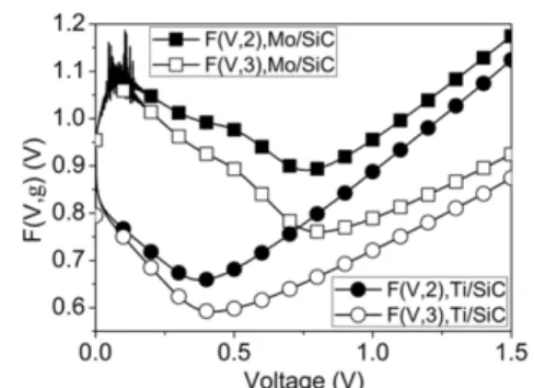
수식에서 열전자방출상수 A**는 4H-SiC에 대한 이론 값에 해당하는 146을 대입하였다[9]. 각각의 수식에 대 하여 dV/ln(J) 그래프의 y절편으로부터 이상계수를, H(J) 그래프의 y절편과 기울기로부터 각각 직렬저항과 SBH를 계산할 수 있다. Norde method에서는는 다음 수식과 같이 정의되는 함수를 통해 소자 특성계수를 산출할 수 있다[10,11].
(5)
일반적인 경우 이상계수는 1 - 2 사이의 값이며 본 연구에서는 2, 3을 적용하였으며, 각 그래프의 최소점 에서의 전압, 전류 및 F(V) 함수 값으로 다음 과정을 통해 소자 특성계수를 계산할 수 있다.
(6)
(7)
(8)
Table 2는 Mo/SiC 및 Ti/SiC SBD의 소자 특성계수를 나타낸다. 각 소자는 일반적으로 알려진 Mo/SiC 및 Ti/
SiC 접합의 SBH 값인 1.2 - 1.3 eV와 0.7 - 0.8 eV와 근사 한 결과를 보였으며, 이들간의 순방향 및 역방향 전류의 차이 또한 SBH의 차이에 상응하는 결과를 나타내었다 [12-14]. 이상계수 또한 1에 근사한 우수한 특성을 나타내 었다. 단일 박막의 경우 4.18Ω/aq.으로 Ti의 22.87 Ω/aq.
보다 낮은 면저항 값을 보인 Mo 가 Mo/SiC 구조의 소 자 제작 시 Ti/SiC 구조보다 높은 직렬저항을 보였다.
이는 보다 높은 값의 SBH로 인해 소자에 흐르는 이상 적인 전류 성분, 즉 쇼트키 장벽을 넘어 이동하는 전자 에 의한 열전자 방출 전류 성분이 제한된 결과이다. 이 상의 결과들로부터 SBD의 전기적 특성에 가장 큰 영 향을 미치는 요인은 금속-반도체 접합에서 형성되는 쇼트키 장벽의 높이이며 대향 타겟 스퍼터링법으로 제 작된 SBD는 이상적인 정류특성에 근사한 전기적 특성 을 보임을 알 수 있다.
4. 결 론
대향 타겟 스퍼터링법으로 제작된 Mo/SiC 및 Ti/
SiC SBD는 이상적인 정류 특성에 가까운 전압-전류 특성을 보였으며, Cheung & Cheung method 및 Norde method를 통해 산출된 소자 특성계수는 각 소자의 전 기적 특성과 상응하는 값을 보였다. 1에 가까운 이상계 수의 값으로부터 제작된 소자의 신뢰성을 확인할 수 있었으며, J-V 특성곡선과의 비교분석을 통해 SBH가 dV
d ln( )J --- nkT
--- Rq +
S
Aeff
J=
H J( ) V nkT ---lnq J
A**T
2
---⎝ ⎠
⎛ ⎞
–
≡
nϕ=
B
+RS
Aeff
JF V γ( , ) V --- kTγ
---lnq I A
eff
A**T2
--- –= 1--- 1γ
n---
⎝ – ⎠
⎛ ⎞V ϕ
B
IRS
---n + +
=
ϕ
B
F V(01
,γ1
) 1 γ1
---- 1n---
⎝ – ⎠
⎛ ⎞V
01
– γ
1
–n---βn –
=
F V(
02
,γ2
) 1γ---- 11
n---⎝ – ⎠
⎛ ⎞V
02
– γ
2
–n---βn –
=
R
S
γ1
–n βI01
--- γ2
–nβI
02
---= =
n γ
1
I02
–γ2
I01
I
02
–I01
---=
V
01
V02
γ2
---- γβ
1
----β – +⎝ – ⎠
⎛ ⎞
F V(
02
,γ2
) F V– (01
,γ1
) V02
γ
2
--- V
01
γ1
--- +
⎝ – ⎠
⎛ ⎞
---
=
Table 2. Devices parameters of Mo/SiC and Ti/SiC Schottky diodes
Device parameter Mo/SiC Ti/SiC
J
F(@1.0V)
[A/cm2
] 0.29 4.02J
L(@5V)
[A/cm2
] 2.00×10⁻¹⁰
1.55×10⁻⁶
φB
[eV] 1.23 / 1.20 0.80 / 0.78R
S
[Ω] 1.44 / 1.43 0.95 / 0.89 n 1.02 / 1.07 1.06 / 1.15(Cheung & Cheung / Norde) Fig. 4. The Norde plots of the Schottky diodes.
30 이진선 · 강태영 · 김경환
반도체디스플레이기술학회지 제14권 제1호, 2015 소자의 전기적 특성에 가장 큰 영향을 미치는 요소임 을 확인할 수 있었다. 이러한 결과들은 우수한 품질의 박막 증착 및 기판, 박막 손상의 억제를 통한 계면 특 성을 확보가 가능한 대향 타겟 스퍼터링법이 SiC 기반 SBD에 적합한 공정임을 시사한다.
감사의 글
본 연구는 미래창조과학부 및 정보통신산업진흥원의 ICT/SW 창의연구과정의 연구결과로 수행되었음 (NIPA-2014-H0502-14-2001).
참고문헌
1. S. K. Gupta, A. Azam, and J. Akhtar, “Improved electrical parameters of vacuum annealed Ni/4H-SiC (0001) Schottky barrier diode,” Phys. B Condens.
Matter, vol. 406, no. 15–16, pp. 3030–3035, 2011.
2. K. V. Vassilevski, I. P. Nikitina, P. Bhatnagar, A. B. Hors- fall, N. G. Wright, A. G. O’Neill, M. J. Uren, K. P. Hilton, A. G. Munday, A. J. Hydes, and C. M. M. Johnson,
“High Temperature Operation of Silicon Carbide Schottky Diodes with Recoverable Avalanche Break- down,” Materials Science Forum, vol. 527–529, no.
1. pp. 931–934, 2006.
3. A. Itoh, T. Kimoto, and H. Matsunami, “High perfor- mance of high-voltage 4H-SiC Schottky barrier diodes,”
IEEE Electron Device Lett., vol. 16, no. 6, pp. 280–
282, 1995.
4. B. J. Baliga, Advanced Power Rectifier Concepts. Boston, MA: Springer US, 2009.
5. B. J. Baliga, Fundamentals of Power Semiconductor Devices. Boston, MA: Springer US, 2008.
6. K. H. Kim, I. H. Son, K. B. Song, S. H. Kong, M.
J. Keum, S. Nakagawa, and M. Naoe, “Thin film properties by facing targets sputtering system,” Appl.
Surf. Sci., vol. 169–170, pp. 410–414, 2001.
7. J. S. Hong and K. H. Kim, “The Performance of IZO Thin Film with Substrate Temperature for OLED Anode,” Journal of the Semiconductor & Display Equipment Technology, vol. 8, no. 3, pp. 51–55, 2009.
8. S. K. Cheung and N. W. Cheung, “Extraction of Schottky diode parameters from forward current-volt- age characteristics,” Appl. Phys. Lett., vol. 49, no. 2, p. 85, 1986.
9. F. Roccaforte, F. La Via, V. Raineri, R. Pierobon, and E. Zanoni, “Richardson’s constant in inhomogeneous silicon carbide Schottky contacts,” J. Appl. Phys., vol. 93, no. 11, p. 9137, 2003.
10. H. Norde, “A modified forward I-V plot for Schottky diodes with high series resistance,” J. Appl. Phys., vol. 50, no. 7, p. 5052, 1979.
11. K. E. Bohlin, “Generalized Norde plot including determination of the ideality factor,” J. Appl. Phys., vol. 60, no. 3, p. 1223, 1986.
12. L. Boussouar, Z. Ouennoughi, N. Rouag, A. Sellai, R.
Weiss, and H. Ryssel, “Investigation of barrier inho- mogeneities in Mo/4H–SiC Schottky diodes,” Micro- electron. Eng., vol. 88, no. 6, pp. 969–975, 2011.
13. T. Nakamura, T. Miyanagi, I. Kamata, T. Jikimoto, and H. Tsuchida, “A 4.15 kV 9.07-mΩ · cm
2
4H-SiC Schottky-barrier diode using Mo contact annealed at high temperature,” IEEE Electron Device Lett., vol.26, no. 2, pp. 99–101, 2005.
14. K. J. Schoen, J. P. Henning, J. M. Woodall, J. A. Coo- per, and M. R. Melloch, “A dual-metal-trench Schottky pinch-rectifier in 4H-SiC,” IEEE Electron Device Lett., vol. 19, no. 4, pp. 97–99, 1998.
접수일: 2015년 2월 26일, 심사일: 2015년 3월 13일, 게재확정일: 2015년 3월 23일