Vol.21, No.1, (2019), pp.10~14 https://doi.org/10.9714/psac.2019.21.1.010
```
1. INTRODUCTION
SQUID is a sensitive detector from magnetic flux to voltage. One recent new application area of SQUID is the amplification of weak radio frequency (RF) signals in the GHz frequency range [1, 2]. We have been developing SQUID-based RF amplifiers for the detection of axion-mediated weak RF signals from a cryogenic microwave cavity. The peak gain of the SQUID RF amplifier should be near the resonance frequency of the microwave cavity. Thus, correct design of the peak gain frequency is important. In the previous study, we designed and fabricated a series of SQUID RF amplifiers, and found that we can predict the resonance frequencies of the SQUID RF amplifiers with acceptable accuracy using a modified model of the resonance frequency [3].
The main performance factors of the SQUID RF amplifier are peak gain at the resonance frequency, bandwidth of the gain curve and noise temperature [4-7].
The gain is mainly determined by the flux-to-voltage transfer coefficient of the SQUID, which is determined by the dynamic resistance of the SQUID at the working point.
The dynamic resistance is the slope in the current-voltage curve with optimum bias current and flux bias of near Φ0/4 (Φ0: flux quantum). This slope is strongly dependent on the hysteresis parameter of the junction (or SQUID), which is again decided by critical current of the junction, shunt resistance and junction size (or junction capacitance). The bandwidth of the gain curve is mainly determined by capacitance of the input coil, such as, linewidth of the input coil line and coupling capacitance at the input pad [5, 8].
* Corresponding author: [email protected]
As the bath temperature of the SQUID RF amplifier chip becomes lower, the noise temperature of the SQUID also decreases. But, if the bath temperature is below around 100 mK, the noise temperature doesn’t decrease further due to hot electron effect of the normal electrons [9].
We designed and fabricated SQUID RF amplifiers with different SQUID parameters and compared the characteristic of the gain cures depending on these parameters to find the optimum combination of SQUID parameters and operation condition.
2. FABRICATION OF SQUID RF AMPLIFIERS
2.1. Design of SQUID RF amplifiers
The basic structure of the SQUID RF amplifier is the same as the standard DC SQUID sensors for measuring low-frequency signals. In the near DC or low-frequency range, the input signal is applied across the two input coil pads. In the RF frequency range, however, the capacitance of input coil generates parasitic resonance and deteriorates the gain performance of the amplifier. Thus, the input coil is used as a microstrip transmission line and one end of the input coil is left open. The resonance frequency of this microstrip amplifier can be calculated using a formula, described in detail in [3].
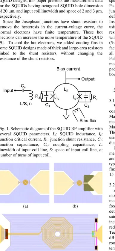
The schematic diagram of the SQUID RF amplifier is shown in Fig. 1. Input RF power is applied to the input coil pads and passes through the coupling capacitor (Cc) to block DC voltage and to adjust the capacitance of the input circuit. A multi-turn input coil with n turns, integrated on the SQUID loop, transfers RF flux to the SQUID. The input coil line has linewidth of L and space S, separated from the
Gain characteristics of SQUID-based RF amplifiers depending on device parameters
Y. H. Lee*,a, K. K. Yua, J. M. Kima, S. K. Leea, Y. Chongb, S. J. Ohc, and Y. K. Semertzidisc
a Ultra-low Magnetic Field Team, Korea Research Institute of Standards and Science, Daejeon, Korea
b Quantum Information Team, Korea Research Institute of Standards and Science, Daejeon, Korea
c Center for Axion and Precision Physics Research, Institute for Basic Science, Daejeon, Korea
(Received 19 January 2019; revised or reviewed 6 February 2019; accepted 7 February 2019)
Abstract
Radio-frequency (RF) amplifiers based on direct current (DC) superconducting quantum interference device (SQUID) have low-noise performance for precision physics experiments. Gain curves of SQUID RF amplifiers depend on several parameters of the SQUID and operation conditions. We are developing SQUID RF amplifiers for application to measure very weak RF signals from ultra-low-temperature high-magnetic-field microwave cavity in axion search experiments. In this study, we designed, fabricated and characterized SQUID RF amplifiers with different SQUID parameters, such as number of input coil turn, shunt resistance value of the junction and coupling capacitance in the input coil, and compared the results.
Keywords: SQUID, radio-frequency amplifier, resonance frequency, amplification gain
SQUID loop (ground) by an insulation layer. The SQUIDs were designed to have different shunt resistance, coupling capacitance and input coil turn numbers for comparison.
The whole SQUID chip has dimensions of 2 mm (W) × 1.7 mm (H), as shown in Fig. 2(a). Among the several SQUID designs, this paper presents the measurement data for the SQUIDs having octagonal SQUID hole dimension of 20 μm, and input coil linewidth and space of 2 and 3 μm, respectively.
Since the Josephson junctions have shunt resistors to remove the hysteresis in the current-voltage curve, the normal electrons have finite temperature. These hot electrons can increase the noise temperature of the SQUID [9]. To cool the hot electrons, we added cooling fins in some SQUID designs made of thick and large-area resistors linked to the shunt resistors, without changing the resistance of the shunt resistors.
Fig. 1. Schematic diagram of the SQUID RF amplifier with several SQUID parameters. Ls: SQUID inductance, Ic: junction critical current, RJ: junction shunt resistance, CJ: junction capacitance, Cc: coupling capacitance, L:
linewidth of input coil line, S: space of input coil line, n:
number of turns of input coil.
(a) (b)
(c)
Fig. 2. Design of the DC-SQUID RF amplifier. (a) Overall chip design without cooling fins, (b) chip with cooling fins, and (c) details of the SQUID loop area with a coupling capacitor, input coil, Josephson junctions and shunt resistors.
2.2. Fabrication of SQUID RF amplifiers
SQUID chips were fabricated on 3-inch Si wafers having resistivity of 10~20 Ω·cm. Standard photolithography method was used for defining the photoresist patterns. All the metal layers were deposited using DC magnetron sputtering with a base pressure of around or below 1×10⁻⁵ Pa. Josephson junction tri-layer is Nb/AlOx/Nb, and junctions size is 2 μm × 2 μm each. The junction area was defined by reactive ion etching (RIE) using SF6 gas.
Insulation layer between metal layers is SiO2 film deposited using plasma-enhanced chemical vapor deposition. Shunt resistors and cooling fin resistors are reliable Pd film. Final wiring layer is 400 nm thick Nb layer, followed by thin (5~10 nm) Pd layer for protection of Nb surface and for facilitating ultrasonic wire bonding. Except for RIE process, all the films were patterned using lift-off process. [10-11].
Fabricated wafers were cut using a diamond sawing machine, and the chip was mounted on an amplifier package with printed circuit board for ultrasonic Al wire bonding.
3. CHARACTERIZATION OF RF AMPLIFIERS
3.1. Current-voltage curves of SQUID RF amplifiers We fabricated a test probe of the SQUIDs with two Cu coaxial cables for RF input and output, respectively, and 8 Manganin wires for DC biases and current-voltage measurement. Fig. 3(a) shows the SQUID package with Manganin wires and a 8-pin connector, and RF connectors.
The SQUID package was shielded again the external noises using an Nb tube having 1 mm thickness, 10 mm inner diameter and 100 mm length, as shown in Fig. 3(b).
Current-voltage (I-V) curves of the SQUIDs were measured by sweeping the bias current through the SQUID and measuring the voltage drop across it. Figs. 4 show typical I-V curves of the SQUID amplifiers with different flux bias. Typical critical current of the SQUID is around 15 μA (at flux bias of near Φ0).
3.2. Gain curve of SQUID RF amplifiers
At a near-optimum bias current with maximum modulation voltage and a flux bias of near Φ0/4, we measured gain curves of the SQUID amplifiers in the frequency range of 1~4 GHz. Since the SQUID operation deteriorates easily at high RF power and also its gain saturates at higher power input, the power level of the incoming RF power was attenuated sufficiently. We reduced the output power of the network analyzer (Agilent Technologies, model E5071C) to its minimum value -55 dBm, and put two attenuators, one 40-dB attenuator at room temperature and 40-dB one at liquid helium temperature. Even though SQUIDs are amplifiers of RF signals, the output signal is still too low to be measured directly by the network analyzer [3, 11]. In ideal low-noise measurements, we need a cryogenic semiconductor RF amplifier based on high electron mobility transistor (HEMT) between the SQUID output and the room-temperature electronics to minimize the nois e
(a)
(b)
Fig. 3. Structure of the SQUID package and test probe for I-V curve and gain curve measurements. (a) SQUID package with DC wiring and connector, and (b) structure of the test probe.
contribution from the room-temperature electronics.
However, the cryo HEMT was not used in this study just for measuring the gain curve of the SQUID RF amplifiers.
Instead, we used two attenuators to prevent the input noises and thermal noise of the room-temperature amplifiers from entering the SQUID. The two 6-dB attenuators were place after the SQUID at 4.2 K and at room temperature, respectively. After the attenuators, room temperature semiconductor amplifiers are followed; HEMT amplifier (Low Noise Factory, LNA-LNR1-15A) and semiconductor amplifier (Miteq, Amp-4F-044050) with a gain of 40 dB and 35 dB, respectively.
3.3. Dependence on the input RF power level
To study dependence of the SQUID gain on the input RF power level, we changed the RF power applied to the SQUID and measured the gain. Fig. 5 shows the SQUID gain versus RF power, where the output power of the network analyzer was changed in a step of 5 dBm. If the RF power at the SQUID input is larger than about -95 dBm, the gain starts to decrease. Therefore, the SQUID input power should be well below -95 dBm. In the following experiments, the RF power was fixed at -135 dBm. If the input RF power is too low, it may introduce large uncertainty in the gain or more noisy gain curve.
(a) (b)
Fig. 4. Typical current-voltage curves of the SQUID. (a) Current-voltage curve with an applied flux near Φ0/2, and (b) current-voltage with an applied flux near Φ0. X-axis is voltage (50 μV/div.) and Y-axis is current (10 μA/div).
Fig. 5. SQUID gain versus RF power level at the SQUID input, where the output of the RF generator (network analyzer) was changed in a step of 5 dBm.
3.4. Dependence on the number of input coil turn
To find the peak-gain or resonance frequency of the SQUID RF amplifiers, we changed the number of turn of the input coil. Fig. 6 shows the change of the resonance frequencies versus number of turns, where other parameters are nearly the same within the controllability of the fabrication condition, such as thickness of the films. We can see that we can control the resonance frequency by changing the number of turn, and the gain increases with increased number of input coil turn [3]. In addition, minor change of the peak frequency can be done by changing the bias current and flux bias point.
Fig. 6. Gain curves of the SQUID RF amplifiers versus numbers of the input coil turn. (a) 20, (b) 19, (c) 18, (d) 17 and (e) 16 turns. Input coil has 2 μm linewidth and 3 μm space.
3.5. Dependence on the shunt resistance
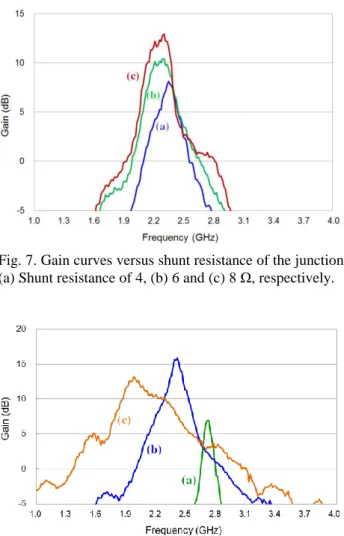
The flux-to-voltage transfer of the SQUID, to which the gain is proportional, increases with hysteresis parameter of the SQUID (βc=2πIcRJ2CJ/Φ0), where Ic, RJ, CJ are critical current, shunt resistance and capacitance of the single junction (see Fig. 1). We changed the shunt resistance and compared the gain curves. As expected, the gain increases as the shunt resistance increases, while the junction remains in the non-hysteretic region.
Fig. 7 shows the gain curves for 3 different shunt resistance values. It shows clearly that larger shunt resistance or larger dynamic resistance in the current-voltage curve gives larger gain at the peak frequency which can be explained by the increase of flux-to-voltage transfer. The hysteresis parameter of the SQUID should be less than 1 to avoid hysteresis in the current-voltage curve. However, due to finite physical temperature (thermal noise) of the SQUID or environmental electromagnetic noise, SQUIDs with hysteresis parameter of slightly larger than 1 also allow stable SQUID operation [12].
Fig. 7. Gain curves versus shunt resistance of the junction.
(a) Shunt resistance of 4, (b) 6 and (c) 8 Ω, respectively.
Fig. 8. Change of gain curve depending on the coupling capacitance in the input coil. (a) Coupling capacitance of 0.1, (b) 0.5 and (c) 1.9 pF, respectively. All the three SQUIDs have the same input coil turn number and shunt resistance.
3.6. Dependence on the coupling capacitance
The inductance and capacitance of the microstrip amplifier determines basically the impedance, quality factor (Q-value) of the resonator, and finally change the gain curve. By adding a coupling capacitor at the input of the input coil, it is possible to change the effective capacitance, and hence the Q-value of the resonator, resulting in change in the gain curve. Fig. 8 shows the gain curves for 3 amplifiers with different coupling capacitances; 0.1, 0.5 and 1.9 pF, corresponding to under-coupling, near critical coupling and over-coupling, respectively [8]. Depending on the coupling capacitance or degree of coupling, the peak gain and bandwidth are shown to be different.
5. CONCLUSIONS
We fabricated SQUID-based RF amplifiers, and compared the gain curves with different SQUID parameters and operation condition. The SQUID amplifier gain saturates if the input RF power is larger than about -95 dBm, meaning that SQUID is really a sensitive amplifier of weak input RF power. The peak-gain frequency of the amplifier can be adjusted by changing the number of turns of the input coil, resulting from the change of input coil inductance or microstrip inductance. As the shunt resistance or hysteresis parameter of the junction increases, the peak gain value increases, resulting from the increase of flux-to-voltage transfer. The shape of gain curves, especially peak gain and bandwidth, changes with the coupling capacitance. Thus, optimum capacitance value can be decided depending on the shape of the gain curve needed.
ACKNOWLEDGMENT
This work was supported by IBS project of CAPP (IBS-R017-D1-2018-a01).
REFERENCES
[1] S. J. Asztalos et al., “Design and performance of the ADMX SQUID-based microwave receiver”, Nucl. Instr. Meth. Phys. Res. A, 656, pp. 39-44, 2011.
[2] S. Michotte, “Qubit dispersive readout scheme with a microstrip superconducting quantum interference device amplifier”, Appl.
Phys. Lett., 94, pp. 122512-1~3, 2009.
[3] Y. H. Lee, K. K. Yu, J. M. Kim, S. K. Lee, Y. Chong, S. J. Oh, and Y. K. Semertzidis, “Correction of Resonance Frequency for RF amplifiers based on Superconducting Quantum Interference Device”, Prog. Supercond. Cryog., 20, pp. 6-10, 2018.
[4] J. Clarke, A. T. Lee, M. Mück and P. L. Richards, “SQUID Voltmeters and Amplifiers”, p. 22-115, Chap. 8, in The SQUID Handbook, Eds. J. Clarke and A. I. Braginski, 2006, Wiley-VCH.
[5] J. Clarke, M. Mück, M. André, J. Gain and C. Heiden, “The Microstrip DC SQUID Amplifier”, p. 473-504, in Microwave Superconductivity, Eds. H. Weinstock and M. Nisenoff, 2001, Kluwer Academic Pub.
[6] M. Mück, and J. Clarke, “The superconducting quantum interference device microstrip amplifier: Computer models”, J.
Appl. Phys., 88, pp. 6910-6918. 2000.
[7] Y. H. Lee, Y. Chong and Y. K. Semertzidis, “Review of low-noise radio-frequency amplifiers based on superconducting quantum interference device”, Prog. Supercond. Cryog., 16, pp. 1-6, 2014.
[8] D. Kinion and J. Clarke, “Microstrip superconducting quantum interference device radio-frequency amplifier: Scattering parameters and input coupling”, Appl. Phys. Lett., 92, 172503, 2008.
[9] F. C. Wellstood, C. Urbina and J. Clarke, Hot-electron effects in metals", Phys. Rev. B, 49, pp. 5942-5956, 1994.
[10] Y. H. Lee, J. M. Kim, K. Kim, H. Kwon, K. K. Yu, I. S. Kim and Y.
K. Park, “64-channel magnetocardiogram system based on double relaxation oscillation SQUID planar gradiometers”, Supercond. Sci.
Technol., 19, pp. S284-S288, 2006.
[11] Y. H. Lee et al., “Development of SQUID-based high-frequency quantum amplifiers”, Annual Report, IBS (IBS-R017-D1- 2016-a01), 2016.
[12] J. Zeng et al., “High intrinsic noise and absence of hysteresis in superconducting quantum interference devices with large Stewart-McCumber parameter”, Appl. Phys. Lett., 103, 042601, 2013.