A Low Power smartRF
Transceiver Hardware Design For 2.4 GHz Applications
Jung-won Kim* , Ung-Se Choi * ★
Abstract
There are many researches to reduce power consumption of battery-operated Transceiver for 2.4 GHz smartRF applications. However, components such as processor, memory and LCD based power managements reach the limit of reducing power consumption. To overcome the limit, this research proposes novel low-power Transceiver and transceiver Hardware Design. Experimental results in the real smartRF Transceiver show that the proposed methods can reduce power consumption additionally than component based power managements.
Keywards: smartRF, UART, SPI, RSSI
Target Markets Applications PC peripherals Mouse, Keyboard, Joystick,
Gamepad
Consumer Electronics TV, VCR, DVD, CD,Remote control Personal Heath Care Monotors, Diagnostics,
Medical Sensors Toy & Games Pets, Games, Educational
* D ept. of Electr onics En gin eerin g, Korea Polytechnic Graduate School
★
Corresponding authorManuscript received Apr. 8, 2008 ; reviced Jun. 25, 2008
I. Introduction
The growing importance of small and cheap wireless devices demands a common platform so that the device can communicate with each other.
With the success of wireless local area networks (WLANs), the wireless networking community has been focused on enhancing WLAN capabilities and developing new approaches to meet the needs of the growing pool of applications requiring wireless devices. Bluetooth [1,2] is an open wireless technology for short-range data communication between moving (or stationary) electronic devices.
So far wireless networking has been mainly focused on high data-rate and relatively long range applications.
Recently, the new concepts of a standardized low data rate wireless personal area networking (LR-WPAN), IEEE 802.15.4 ZigBee, smartRF has been emerged in the frequency band of 2.4 GHz [3,4,5]. Table I summarizes the target markets and applications of smartRF standard.
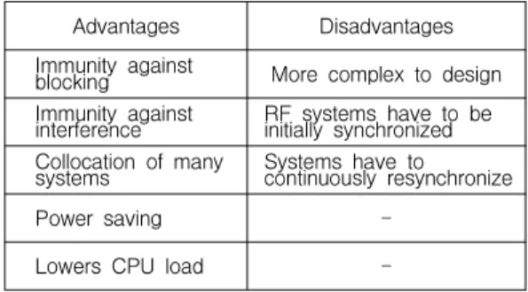
Table 1. Markets & Applications of smartRF
Advantages Disadvantages Immunity against
blocking More complex to design Immunity against
interference RF systems have to be initially synchronized Collocation of many
systems Systems have to continuously resynchronize
Power saving -
Lowers CPU load -
As shown in Table I, there are so many applications for this low date rate standard such as industrial and commercial, home automation, personal computer peripherals, consumer electronics, personal health care, toys and games that should be able to operate for six months to two years in just button cells or batteries [6].
There are several works on low power 2.4 GHz transmitter that have been reported in literature [7,8]. However, those works still consume high power. With the motivation of low power, high linearity to fulfill the demand of new trends, this paper presents a low-power Tranceiver Hardware Design for 2.4 GHz smartRF technology. The Frequency Hopping method is described in Section II. Section III presents the practical Hardware design. The experimental results are shown in Section IV and Section V concludes this work.
II. Frequency Hopping
The advanced RF firmware includes two hopping modes: no hopping (always the same channel) and a random-based hopping scheme. The advantage of a frequency hopping system is that the designed RF system is much more robust with respect to interference and the blocked or disturbed channels.
Another advantage is the collocation of many different systems in the same range. To get a working link it is useful to separate the different participants of the whole RF system by channel and time. This makes it necessary to synchronize all RF systems of one link by channel and time. Frequency hopping also increases the system performance, as the RF task only has to be activated during specific time slots, lowering power consumption to a minimum. A disadvantage of such systems is that if the synchronization of time and channel is lost, then the RF link is destroyed and has to be set up again. Table 2-1 gives an overview of the advantages and disadvantages of a frequency
hopping spread spectrum (FHSS) system.[9]
Table 2. The advantages and disadvantages of frequency hopping
To improve the system even more, the firmware takes a further random number. This random number is placed in the address field of the RF packet. The RF firmware takes only two random numbers, one for calculating the hopping scheme and one is used as a random address for the system. If the user wants to collocate many systems in the same range, then the system should be made more random or adaptive. Of course, we have only been discussing the separation by channel, but the different systems are also separated by time. This means that even if two different systems use the same channel, then a collision of data is very unlikely, as they are also separated by time.[10]
To design a suitable RF link regarding the hopping scheme in use, some calculations have to be done to determine the probability that two systems the same random-based hopping algorithm.
It is hard to say how small this number should be, but the smaller it is, the better.
III. Usable Peripheral Interfaces
There are two peripheral interfaces which can be used to serve the RF transmit task and the RFreceive task: a UART interface and an SPI interface. Each has advantages and disadvantage, to decide which is the better solution, the system design and the sub-tasks of the whole system have to be considered.
III-I. SPI Interface
For the transmission of RF data, there is no problem using the SPI. The RF data is simply writtento the SPI data register and then transferred to the transceiver. The only potential problem in this case is that the RF data stream must not be interrupted by gaps created by the data handling of the SPI, such as is possible if the SPI is not double buffered. Carefully written software can protect against this failure.
The reception of RF data via the SPI is, however, a much more complex task, as the synchronization of the incoming RF data has to be handled by software. This requires code space and, therefore, CPU cycles. Once synchronization is done, the reception of a data packet is easy, as long as the software is able to read the SPI data register fast enough to prevent a possible buffer overrun; as most microcontrollers use a double buffered SPI for receiving data, this should not be difficult.
III-II. UART Interface
For transmission, it is easy to use the UART interface. The RF Data is simply written to the UART data register and then transferred to the transceiver. The only potential problem is that the RF data stream must not be interrupted by gaps created through the data handling by the UART.
This can easily occur if the UART is not double buffered in transmit mode. As when using the SPI interface, these gaps can be avoided with well-written software. However, since most microcontrollers contain a double-buffered UART,
this issue will be only a theoretical one.
The reception of RF Data via the UART is also not complex, as the synchronization on the incoming RF Data is handled by hardware. This is a convenient method for designing a receiving interface to the transceiver, as no additional code or CPU performance is required. The only concern is to design software that is able to read the UART data register fast enough to prevent a possible buffer overrun of the peripheral. As most of the controllers use a doublebuffered UART for receiving data this should be no problem.
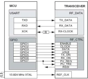
Ⅳ. Hardware Concept Design
To exchange data via RF, the chips are connected via the USART interface of the microprocessor (Figure 3-1). To achieve the high data rate of 1.152 Mbps, the USART is used in synchronous mode, requiring the pin XCK. This pin is used for sampling the incoming data from the Transceiver.
In transmit mode (as seen from the Transceiver) data is shifted out from the microprocessor TXD pin into the TX_DATA pin of the Transceiver. In this case the pin XCK is configured as output.
Figure 4-1. Hardware Concept
As this would collide with the output pin
CLK_REC of the Transceiver, a series resistor has to be put in this connection line. Also, the USART is configured in the MPC (Multi-processor Communication) Mode, a special mode that can be used to realize an automatic detection of a valid RF address while using only a minimum of CPU power.
To transmit one byte of payload, three bits have to be added (start bit, stop bit and MPCM bit), giving each byte of data a transmit length of 11 bits and lasting (at a data rate of 1.152 Mbps) for 9.56 μs.
Configuring the Transceiver is done via an SPI-like three wire interface (Clock, Data, Enable). Via this configuration, the Transceiver is settled on the desired channel. As a special feature the Transceiver has a programmable Gaussian filter, active only during the transmission of a data packet. The configuration word length is 16 bits for transmit and 25 bits for receive. The other control lines control the behavior of the RF chip.
The Transceiver offers the possibility of evaluating an RSSI signal. This analog signal indicates the strength of the incoming RF signal and can, for example, be used to trigger the microprocessor internal analog comparator to enable the USART. The analog comparator should be used to obtain a quick response on the start of an RF data packet; however, if an exact value of the RSSI voltage is required, it is easy to pass the RSSI to the ADC via an microprocessor internal multiplexer.
To evaluate the RSSI with this ADC needs much more time, of course, than doing the same with the analog comparator. The RF firmware does not use this feature because it is a system which is synchronized (that is, all the devices of the whole RF system are synchronized to the master). Using the ADC to evaluate the RSSI will decrease the sensitivity of the system. In systems that are not synchronized it is very helpful to have such an RSSI signal, as it can trigger the receiver to enable the reception of the RF packet.
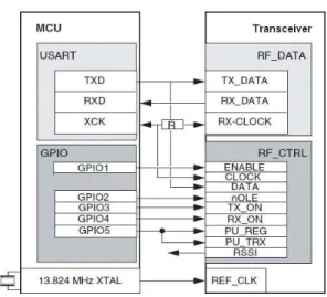
Figure 4-2. Improved Hardware Concept
Another advantage of the whole RF system is that only one crystal is needed (at a frequency of 13.824 MHz). This crystal is connected to the microprocessor and the output is passed to the ISM transceiver chip. It is very important when starting the development of application software to have the correct settings of the microprocessor internal fuse bits (CKOPT fuse has to be set to have the full swing signal of the crystal). In order to reduce the I/Os needed to control the transceiver, some of the lines are connected together as shown in Figure 4-2.
V. Experimental Results
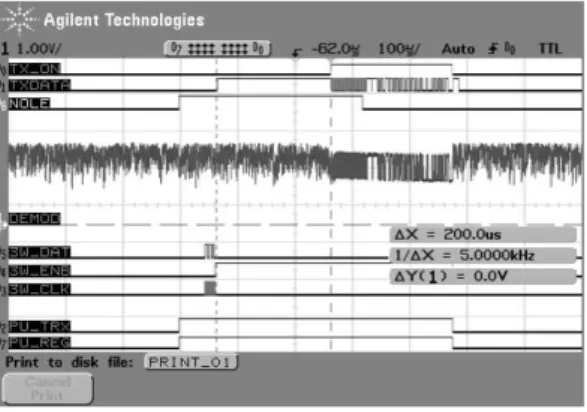
Figure 5-1 shows the transmitted signal which is received by a reference receiver.
Starting from power down mode, U_REG &
PUTRX are toggled to high about 40us in advance to 3-wire programming. After performing the 3-wire programming (PLL and Deviation) the loop needs to settle frequency. TX_ON is toggled to high about >200us after the PLL - progra mming.
Open-Loop-Enable (nOLE) toggles at start of modulation (TX_DATA) – which takes place about 50us after toggling TX_ON to high.
Figure 5-1. TX-Timing Measurement
It is recommended to start sending a preamble already at TX_ON. When the TX-Burst is finished, all signals can toggle to low and the IC returns back to power down mode.
The RX-Timing is similar to the TX-Timing – starting from power down mode, PU_REG &
PU_TRX are toggled to high about 40us in advance to 3-wire programming. After performing the 3-wire programming (PLL and optionally Clock-Recovery), the loop needs to settle frequency.
RX_ON is toggled to high about 150μs after PLL-programming. Open-Loop-Enable (nOLE) can be kept high because receiving is also possible at closed-loop mode.
Fig. 5-2 shows the measured result of RSSI versus RF-level at Receiver Input and obtained result RX_IN Sensitivity is -91 dBm easured performances.
Figure 5-2. RSSI versus RF-level at Receiver Input
Ⅵ. Conclusion
This work presents a low voltage low power RF Transceiver Hardware Design for 2.4 GHz smartRF module. Transmitting data with the Transceiver is not difficult in principle since data is simply shifted out bit-per-bit and then transmitted via the air.
There are two important things that have to be considered, though.
The first is that the data shifted into the Transceiver has to be synchronous; this means each bit going into the Transceiver must have a duration of multiples of 868.055 ns (n × 0.868055 ns).
The second point is that no gaps between the bytes of the data stream should occur. Receiving the RF data is much more complex, as the receiving system has to be synchronized to the incoming RF data stream. This means the system must be able to find the first valid bit in the incoming RF data packet. That is one of the most important tasks regarding an RF link. Low cost of program memory and CPU performance to implement a robust and powerful RF link.
References
[1] IEEE 802.15.4/D18, Low Rate Wireless Personal Area Networks, std. 2003.
[2] J. Zeng et al., “Will IEEE 802. 15 .4 Make Ubiquitous Networking a Reality? : A Discussion on Potential Low Power, Low Bit Rate Standard,” IEEE Communications Magazine, vol. 42, pp. 140-146, June 2004.
[3] P. Choi et al., “An Experimental Coin-Size Radio for Extremely Low-Power WPAN (IEEE 802.15.4) Application at 2.4 GHz,” IEEE Journal of Solid-State Circuits, vol. 38, pp 2258-2268, December 2003.
[4] B. Razavi, “Design Considerations for Direct Conversion Receivers”, IEEE Transactions on Circuits and Systems-II: Analog and Digital Signal Processing, vol.44, no.6, pg.428-435, June 1997.
[5] K. T. Christensen, Low Power RF Filtering For CMOS Transceiver, Ph.D Dissertation, Technical University of Denmark, 2001.
[6] T. Nguyen et al., A Low Power CMOS RF Transmitter Front - end For 2.4 GHz ZigBee Applications
[7] Chee Kheong Siew and David J. Goodman,
“Packet Data Transmission Over Mobile Radio Channels”, Transactions of IEEE vehicular technology, vol.38, May 1989.
[8] Patrick Kinney Kinney Consulting LLC Chair of IEEE 802.15.4 Task Group Secretary of ZigBee BoD Chair of ZigBee Building Automation Profile WG [9] Anuj Batra et al., Proposal for Intelligent BT Frequency Hopping for Enhanced Coexistence, IEEE 802.15-01/082, January 2001.
[10] Matthew B. Shoemake, Ph.D., Wi-Fi (IEEE 802.11b) and Bluetooth Coexistence Issues and Solutions for the 2.4 GHz ISM Band.
BIOGRAPHY
Jung-won Kim (Member)2002 : BS degree in Electrical Engineering, Korea Polytechnic University.
2004 : MS degree in Electrical Engineering, Korea Polytechnic University.
2008 : PhD courses at Electrical Engineering, Korea Polytechnic University.
2001~2004 : Research Engineer, Namsong Ind.
2004~ : Research Engineer, Changnam I.N.T
Ung-se Choi (Member)
1981 : BS degree in Electronics Engineering, Myong-Ji University.
1983 : MS degree in Electronics Engineering, Myong-Ji University.
1995 : PhD degree in Electronics Engineering, Myong-Ji University.
1981~1997 : Advanced Research Engineer, KITECH.
1997~ : Professor, Department of Electronics Enginnering, Korea Polytechnic University