- 1370 -
산업용 가속기용 고출력 펄스시스템의 설계와 시험
장성덕* & **, 김상훈*, 양해룡*, 조무현*, 고인수*, 남궁원* 포항공과대학교* , 포항 가속기연구소**
Design and Test Results of High-Power Pulse Generator System for Industrial Accelerator Application
S. D. Jang* & **, S. H. Kim*, H. Y. Yang*, M. H. Cho*, I. S. Ko*, and W. Namkung* POSTECH*, PAL**
Abstract - A conventional linear accelerator system requires a flat-topped pulse with less than ± 0.5% ripple to meet the beam energy spread requirements and to improve pulse efficiency of RF systems. A a line-type pulsed modulator is widely used in pulsed power circuits for applications such as accelerators, radar, medical radiation, or ionization systems. The high-voltage pulse generator system with an output voltage of 284 kV, a pulse width of 10 ㎲, and a rise time of 0.84 ㎲ has been designed and fabricated to drive a klystron which has 30-MW peak and 60-kW average RF output power. The high-voltage test was performed using the klystron load.
This thesis describes the design and test results of high-power pulse generator system for industrial accelerator application. The experimental results were analyzed and compared with the design.
I. INTRODUCTION
An industrial linear accelerator system for E-beam sterilization is under development for bio-technology applications. It can be used to improve the properties of macromolecular materials or to sterilize medical equipment and farm products. This accelerator system requires a flat-topped pulse with less than ± 0.5% ripple to meet the beam energy spread requirements and to improve pulse efficiency of RF systems.
In the linear accelerators, a pulse modulator system with a line-type PFN can be used to drive a high-power klystron as a pulsed RF source amplifier. The pulse modulator with a pulse width of 10 ㎲, a rise time of 0.84
㎲, and a pulse droop of 2.9% has been designed and tested to drive a klystron which has an output voltage of 284 kV, 30-MW peak and 60-kW average RF output power. In this paper, the pulse generator system was investigated and analyzed with the pulse response characteristics using a simplified equivalent circuit model. the pulse rise characteristics are simplified and generalized for a high-power klystron. The practical limitations on the rise time are discussed. The experimental results are analyzed and compared with the design.
II. DESIGN BACKGROUNDS A. Equivalent circuit analysis
A pulse transformer and its associated pulse generator and load can be represented by an equivalent circuit.
Pulse Transformer Lw
CD
LP
RE
RG
+-
Load VG
RL
LL
CL
Pulse Generator SG
VG: Charging Voltage of PFN SG: Thyratron Switch RG: PFN Impedance LW: Wiring Inductance
LL: Leakage Inductance RE: Core Resistance LP: Primary Inductance CD: Distributed Capacitance
CL : Load Capacitance RL: Klystron Impedance
Fig. 1. Equivalent circuit of pulse generator system
Figure 1 shows the equivalent circuit of a pulse generator, step-up pulse transformer and load.
[1-3]By analyzing the behavior of each of simplified equivalent circuits for a given pulse width (τ) and load (R
L,C
L), transformer parameters such as primary inductance (Lp), leakage inductance (L
L), distributed capacitance (C
D) can be determined and thereby optimized for the best pulse response. These transformer parameters are a function of coil geometry and winding configuration, dielectric constant of the insulation, and the permeability of the core material.
B. Optimum waveform and rise time analysis
The pulse efficiency depends on the detailed design parameters of the pulsing system including a pulse transformer and a load. We can neglect the effect of the shunt resistance R
eand the shunt inductance L
Pduring the short rise time in the leading edge analysis.
The normalized load voltage y(t) defined as
(1)
is given by
(2)
≧ (3)
where a = 2 πσ
τ , k = 2 π σ
2- 1
τ , ω = 2 π 1 - σ
2τ
σ = 1
2 π m ( m + 1) { γ m + 1 γ } , τ = 2 π ( m + 1) m L
TC
Tm = R
LR
G, γ = Z
TR
L, Z
T= L
TC
TL
T= L
W+ L
L, C
T= C
D+ C
Lm : matching parameter between the generator and the load, and γ is the impedance matching parameter between the transformation system and the load, Z
Tis the transformation impedance of the pulsing system.
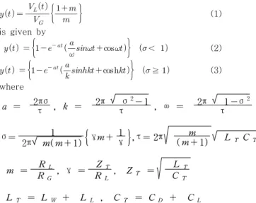
The expanded view of the leading edge of y(t) near the flat top is shown in figure 2 as a function of the damping factor σ. In this figure, the normalized time S is defined by S = t/τ . For a given value of L
Tand C
T, small σ gives fast rise time but generates large overshoot. For a matched load, the rise time is determined by
(4)
where, S (σ) is a fitting function to give the rise time from 10% to 90% of maximum pulse height.
2009년도 대한전기학회 하계학술대회 논문집 2009. 7. 14 - 17
- 1371 -
0 .9 5 0 .9 6 0 .9 7 0 .9 8 0 .9 9 1 .0 0 1 .0 1 1 .0 2 1 .0 3 1 .0 4 1 .0 5
0 .0 0 .2 0 .4 0 .6 0 .8 1 .0 1 .2 1 .4 1 .6 1 .8 2 .0 S
y(t)
σ = 0 .7 σ = 0 .8
σ = 0 .9 σ = 1 .0
σ = 1 .1 σ = 1 .2
Fig. 2. Normalized rising-pulse waveform for various values of the damping factor
In general, a pulse flat-top with less than ± 0.5%
ripple is required to produce a high efficiency pulse. The damping factor σ has to be larger than 0.86 to limit the overshoot to less than 0.5% during the flat-top.
[4]From the above analysis, a fast rise time can be realized by reducing the number of secondary turns, but it produces larger pulse droop and core size. Thus, tradeoffs among these parameters is required to generate the optimum output pulse.
[5]C. Pulse generator design
The pulsed-power generator has a pulse-forming network (PFN), a high-power pulse switch, and a step-up pulse transformer. The design procedure of a pulsed generator system is summarized in Fig. 3.
Fig. 3. Design procedure of a pulsed generator
The total capacitance of the PFN is given by the principle of energy-conservation. The energy stored in the PFN must be the same as the energy transferred to the load by a pulse:
2 0
1 2
Tp
PFN PFN L
L
C V = ∫ V I dt (5)
or
2
2
L L P PFNPFN
V I T C = V
(6) where
C
PFN= the total PFN capacitance V
PFN= the charging voltage of the PFN T
P= the pulse width
V
L= the load voltage I
L= the load current
The total inductance of the PFN, L
PFN, is given by the equation for the PFN characteristic impedance Z
PFN:
PFN PFN
PFN
Z L
= C
(7)
The number of sections of the PFN, N
PFN, is closely related to the pulse rise time and to the required flatness of the pulse top. In general, a larger section gives a faster rise time.
III. SYSTEM DESCRIPTION
The pulse generator with the high-voltage pulse transformer is used to drive a 30-MW klystron for a 10-MeV electron beam accelerator system. The main electrical circuit diagram and design parameters of the pulse generator are shown in Fig. 4. Main components of this system are composed of 15-stages of PFN, thyratron tube switch (E2V, CX2412X), 1:13 step-up pulse transformer.
Fig. 4. Schematic circuit diagram of a pulse generator In this system, the pulse energy is initially stored in an artificial delay-line PFN and then periodically discharged into the primary of the pulse transformer by a thyratron switch. During the inter-pulse period, the PFN is recharged from the dc supply.
IV. EXPERIMENTAL RESULTS A. High voltage test
The high-voltage performance test was performed with a klystron (TV2022D S/N: 23187) to measure the pulse characteristics of the pulse generator by using the circuit layout as shown by Fig. 4. In the circuit, the PFN capacitor was charged to a voltage of 42 kV by using a high-voltage inverter power supply. Initially, the pulse modulator was tested with a 6.51 Ω resistive matching load, which is equivalent to klystron impedance referred to the primary of the pulse transformer. By tuning the PFN inductance, the output voltage of the pulse modulator was set to the desired rise-time and flat-topped pulse. The final test conditions and results for high-voltage performance measurement are summarized in Table 1.
Table 1. HV test conditions and results
Test Parameters Values
Klystron load 1.1 kΩ
PFN charging voltage 42 kV
Load beam voltage (V
B) 276.58 kV Load beam current (I
B) 246.4 A
Pulse width@70% (T
p) 9.3 ㎲
CVD ratio 11,500
CT ratio 0.05 V/A
- 1372 -
Figure 6 shows a set of displays of the final-load voltage and the corresponding current. As a result, the high voltage pulse with a rise time of 0.85 ㎲ (10-90%) was successfully generated up to 277 kV at a frequency of 10 Hz. The pulse width of the output voltage is 9.3 ㎲ with a flat-top of 6.5 ㎲ and a flatness of 1.3%. From the measured waveform analysis for klystron, the measured rise time is confirmed as 1.4 ㎲ (0-99%) with an overshoot of 2%, and the pulse droop approximately 2.7%.
Time [2μs/div.]
277 kV
Load beam voltage
Load beam Current
246.4 A
Time [2μs/div.]
277 kV
Load beam voltage
Load beam Current
246.4 A
Fig. 6. Output voltage (11,500X) and current (20X) waveform with the klystron
From the measurement data using the klystron, we can find the differences both overshoot of 1.5% and voltage droop of 0.3% with the design. In this test, the PFN inductance was not adjusted to tune a flat-top and optimize the output waveform. Subsequent experimentation is needed to accomplish this. The droop can be compensated by PFN tuning. The large overshoot can be reduced by tuning the damping factor σ with wiring inductance.
B. Simulation and discussion
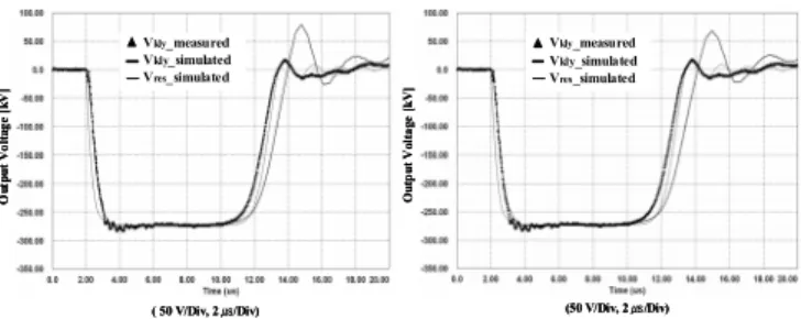
To investigate the parameter value to be matched with measured result, the simulation method was used to analyze the behavior of the equivalent circuit model. Fig. 7 shows the simulation circuit and parameters of the pulsed modulator system using the Psim 7.05 code.
Fig. 7. Simulation circuit of the modulator system After assigning all the known parameters and estimating values for the devices, the PFN inductors are tuned to generate an optimum pulse output. The characteristics test results of the pulse system were compared with those of a simulated circuit, and the both results were found to be in agreement. Figure 8 presents the tested and simulated waveforms for the klystron cathode voltage. In both (a) and (b), the triangle curve (V
kly_measured) is the measured waveform and the thinner curve (V
res_simulated) is the simulated waveform for a resistive load of 6.51 Ω without PFN tuning at 2
μH. The simulated waveform for a resistive load gives the even flat-top width without overshoot, but the measured waveform shows an overshoot of approximately 2%.
( 50 V/Div, 2 ㎲/Div)
Output Voltage [kV]
(50 V/Div, 2 ㎲/Div)
Output Voltage [kV]
Vkly_measured Vkly_simulated Vres_simulated
Vkly_measured Vkly_simulated Vres_simulated
( 50 V/Div, 2 ㎲/Div)
Output Voltage [kV]
(50 V/Div, 2 ㎲/Div)
Output Voltage [kV]
Vkly_measured Vkly_simulated Vres_simulated Vkly_measured Vkly_simulated Vres_simulated
Vkly_measured Vkly_simulated Vres_simulated Vkly_measured Vkly_simulated Vres_simulated