Nomenclature
η: conversion efficiency of solar cell, % J sc : short-circuit current, mA/cm 2 V oc : open-circuit voltage, V FF: fill factor, %
R sh : shunt resistance, Ω·cm 2 R s : series resistance, Ω·cm 2
Subscript
Se/M: Se/metal ratio CGI: Cu/(Ga+In) ratio GGI: Ga/(Ga+In) ratio PDT: post deposition treatment
1. Introduction
Cu(In,Ga)Se 2 (α-CIGS) solar cells with a ban gap of 1.2 eV have received a great deal of attention due to their long-term stability in outdoor conditions and high absorption coefficient.
The efficiency of α-CIGS solar cells is as high as 22.6-22.9% 1, 2) . The Cu(In,Ga) 3 Se 5 (β-CIGS) phase is often found on the surface of the α-CIGS film because of excess supply of In, Ga, and Se during the three-stage co-evaporation process 3-5) . The existence of this phase greatly enhances the device performance of the CIGS solar cell 6, 7) . It is seen that an epitaxial surface layer with an intrinsic β-CIGS phase prevents surface recombi- nation by reducing the valence band maximum downward at the CIGS surface.
β-CIGS material with a band gap of 1.34 eV has potential for higher efficiency than that of α-CIGS material with a band gap of 1.2 eV according to the Shockley-Queisser limit. However, the cell efficiency with a β-CIGS light absorber was below 15%
even though the band gap of β-CIGS was favorable compared to α-CIGS light absorber.
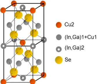
Fig. 1 shows the tetragonal crystal structure of the β-CIGS
3