power consumption of the pixel array. In addition, the computation circuit for a block-based CIS is very flexible for various types of pixel structures. The proposed CIS was designed and fabricated using a standard CMOS 0.18µm process, and the performance of the fabricated chip was evaluated. From a resultant image, the proposed block-based CIS can calculate a differing contrast in the block and control the operating voltage of the unit blocks. Finally, we confirmed that the power consumption in the proposed CIS with a simple pixel structure can be reduced.
Keywords: CMOS image sensor, Low-power image sensor, Active pixel sensor
1. INTRODUCTION
A charge-coupled device (CCD) and a complementary metal- oxide-semiconductor (CMOS) image sensor (CIS) are commonly used for image capture [1-7]. Recently, CISs have mainly been used for portable devices and security cameras because a CIS is cheaper and more power efficient than a CCD-type image sensor [8-10]. The operation of most portable devices depends on battery power. Because battery power is limited, it is essential that most devices consume less power. In recent years, many studies have been conducted to develop low-power CISs [11,12].
Major studies on low-power CISs focused on low-operation voltage for the supply voltage of a device, methods for including variable frames by controlling the integration time in the CIS, and obtaining a computation pixel signal level [13-16]. The method used to obtain low-operation voltage is very difficult to design into a CIS chip. Low-operation voltage only depends on the CMOS process. In addition, the output voltage swing in the pixel is
important for reducing the noise level; the supply voltage for a pixel is somewhat large. Establishing a variable frame rate by controlling the integration time creates a problem: different levels of brightness at different integration times.
We propose a block-based low-power CIS that clearly improves pixel power efficiency. By using an additional computation circuit, the proposed CIS improves the area efficiency and can use the conventional structure of a three-transistor active pixel sensor.
Previous work also proposed block-based CISs, but the complex pixel structure was composed of one photodiode, eight transistors, and twelve signal lines [17]. Those designs also included a small photodiode and had a low fill factor. We propose a new type of block-based CIS that has one photodiode, three transistors, and six signal lines. Not only can we create a simple pixel structure, but we can also improve the fill factor in the pixel.
The proposed block-based CIS was implemented in a 0.18 ìm standard CMOS process on a Cadence Virtuoso platform, and was simulated in Cadence Spectre.
2. EXPERIMENTAL
2.1 Design of proposed CIS
The proposed CIS structure is shown in Fig. 1. The block-based system consists of a unit block, a winner-take-all circuit, a loser- take-all circuit, an update circuit, a subtractor, a comparator, and a static random-access memory (SRAM) cell. Each unit block is
1School of Electronics Engineering,
2Department of Sensor and Display Engineering,
Kyungpook National University, 1370 Sankyuk-dong, Buk-gu, Daegu 702- 701, Korea
+Corresponding author: [email protected]
(Received: Jan. 2, 2014, Revised: Feb. 25, 2014, Accepted: Feb. 26, 2014)
This is an Open Access article distributed under the terms of the Creative Commons Attribution Non-Commercial License(http://creativecommons.org/
licenses/bync/3.0) which permits unrestricted non-commercial use, distribution, and reproduction in any medium, provided the original work is properly cited.
composed of 4-by-4 pixel arrays. The output of each row pixel becomes the inputs of the winner-take-all and loser-take-all circuits. The difference in brightness is calculated by the outcomes of the winner-take-all and loser-take-all circuits. The winner-take- all/loser-take-all cells calculate the maximum and minimum output of each row of pixels separately. The update circuit calculates the maximum and minimum outputs in the unit block output, and the maximum output is subtracted from the minimum output by using a subtractor circuit. The output signal of the subtractor is the difference in darkness in the unit block. The difference in darkness is compared to the reference signal by using the comparator. Therefore, the input to the SRAM is a digital signal, which is stored. Finally, the unit block operates according to the stored signal state in the SRAM.
2.1.1 Design of the unit block and pixel
The design of the unit block is very important for the operation of a block-based system with a simple pixel structure. The proposed unit block and pixel structure are shown in Fig. 2. The unit block cell is composed of 4-by-4 pixel arrays. All pixels consist of one photodiode, four transistors, and include three signal lines and two power lines. The drain node, M1, in the pixel is connected to the VCONTROL node. The VCONTROL node controls each block from the computation result. Further, the initial condition of the VCONTROL node is set to high. Briefly observing the operation of the pixel, after integration time from reset, the read operation is performed sequentially from 1 row. Each pixel signal of 1 row is transmitted to the winner-take-all and loser-take-all process in the computation circuit. Then, the next rows are successively transferred to the winner-take-all/loser-take-all process.
2.1.2 Design of the computation circuit
The computation circuit is composed of the winner-take-all/
loser-take-all circuit, the update circuit, the subtractor, the comparator, and the SRAM cell.
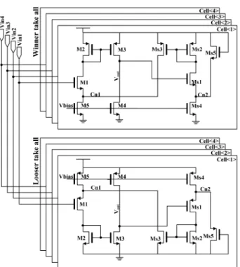
The winner-take-all/loser-take-all circuit structure is shown in Fig. 3. Cells from the winner-take-all and loser-take-all process are compared to each Vin of the unit cells, resulting in a digital signal [18]. The input voltage of the winner-take-all cells is converted into current by M1. The currents of M1 are compared to other currents in the Cn1 and Cn2 nodes. Each Vout signal is converted into a digital signal, which is either “0” or “1.” Digital signals select their maximum values by using a switch. The loser- Fig. 1. Structure of proposed block-based CIS.
Fig. 2. Structure of unit block composed of a three-transistor active pixel sensor.
take-all circuit also has a digital signal for the minimum signal.
The winner-take-all/loser-take-all circuit transmits the maximum and minimum output voltages in each row of pixels to the update circuit.
The circuit structures of the winner update, loser update, and proposed subtractor are shown in Fig. 4. The operation methods of the winner update and loser update are used in a similar manner in both Fig. 4 (a) and 4(b). When the S1 signal is applied, the comparator compares the winner and loser signals to the update node signal. The S2 signal is applied next, and the winner or loser
signal is updated to the capacitor from the previous result of the comparator. After updating the maximum and minimum signals from the unit block, the winner and loser update nodes are transmitted to the two inputs of the subtractor circuit separately.
Previous subtractor circuits consisted of an operational amplifier and four resistors. In those previous subtractor structures, the current consumed by the operational amplifier was more than the current consumed in our proposed structure. In addition, using four resistors presented a problem in the consumed chip area. Therefore, we propose a simple structure for the subtractor design of three switches and one capacitor, as seen in Fig. 4. When the D1 signal sends an initial sampling to the capacitor, the capacitor stores the Vin1 signal. The D2 signal operates the next sampling, where Vout shows the Vin1 – Vin2 signal. The result of the subtractor is transmitted to the comparator, and the Vin1 – Vin2 signal is compared to the reference signal using the comparator in Fig. 1. Next, the result of the comparator is stored in the SRAM cell. The digital signal in the SRAM drives the control signal in the unit block (VCONTROL in Fig. 2).
2.2 Simulation
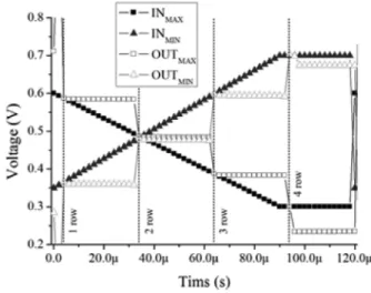
We simulated a computation circuit using Cadence Spectre with a simulation library of standard 0.18µm CMOS processes. The simulation results of the winner-take-all/loser-take-all circuit are shown in Fig. 6. The common input voltage range of the winner- take-all/loser-take-all circuit is set to the output swing of the pixel in Fig. 6 (a). The winner-take-all/loser-take-all circuit selects the maximum and minimum signals in the unit row in Fig. 6 (b).
Although the winner-take-all and loser-take-all circuits have a problem in that the maximum resolution is limited to about 63 mV, the winner-take-all and loser-take-all are only used in computation mode and are just compared with the reference Fig. 3. Structure of the winner-take-all and loser-take-all circuits.
Fig. 4. Structure of (a) winner update and (b) loser update circuits.
voltage (normally 200 mV). Fig. 6 (c) shows the worst resolution of the winner-take-all circuit. When the input voltage is nearly 0.7 V, the worst resolution is about 63 mV. Fig. 7 shows the simulation results of the update circuit. According to the winner
update and loser update circuits in Fig. 4, INMAX and INMIN represent the winner and loser nodes, and OUTMAX and OUTMIN represent the winner update and loser update nodes, respectively.
The voltage range of the two inputs is the output voltage swing of the pixel; INMAX and INMIN are increasing and decreasing, respectively. Therefore, the OUT node is updated by comparing the OUT node to the IN node.
3. RESULTS AND DISCUSSIONS
3.1 Measurement environment
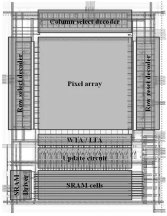
The layout of the proposed chip is shown in Fig. 8. The proposed chip consists of a pixel array, decoders, and additional computation circuits for operating a block-based structure. The proposed chip was implemented in a Magnachip/SK Hynix 0.18 ìm standard CMOS process. Because it was not implemented by using the CIS process, the proposed chip was expected to have a lower image quality than that if we had used the CIS process.
Therefore, we focused on an additional circuit for operating a block-based CIS.
In order to measure the proposed block-based CIS, we designed a printed circuit board (PCB). Fig. 9 shows the blueprint of (a) the chip mount PCB and (b) the controller PCB. The completed module for measurement is shown in Fig. 10. The operating digital waveform is shown in Fig. 11. The signals of S1 and S2 are used to control the update circuit. D1, D2, reset, and WR are also used to control sequence circuits. To operate the block-based CIS, we produced an operating signal by using Verilog hardware description language (HDL) code with a field-programmable gate array (FPGA).
Fig. 6. Simulation results of winner-take-all and loser-take-all: (a) Common input signal, (b) output signal from winner-take-all and loser-take-all circuits, and (c) worst resolution of winner- take-all circuit.
Fig. 7. Simulation result of the update circuit.
3.2 Measurement results
Fig. 12 shows the measurement results of (a) the original image and (b) the block-based CIS when the lens aperture is changed from closed to open. Fig. 13 shows the measurement results when the reference voltages are (a) 440 mV, (b) 573 mV, (c) 683 mV, and (d) 713 mV. We can capture images by controlling the aperture and reference voltage, and the proposed block-based system can determine the difference in brightness in the unit
block. It was possible to confirm that, in response to reference voltage, the shape of the block is chrranged, although the resulting image shows a noise factor.
Fig. 8. Layout of the proposed block-based CIS.
Fig. 9. Blueprints of the (a) chip mount PCB and (b) controller PCB.
Fig. 10. (a) Side view and (b) front view of the completed mea- surement system.
Fig. 11. Operating digital waveform for calculating a signal of period of each block.
3.3 Discussion
The proposed block-based CIS has a simple pixel structure for unit blocks. Therefore, we can use a photodiode with a relatively large area. The number of transistors and signal lines are summarized in Table 1, with respect to the type of pixel. The proposed pixel structure is simpler than the previous pixel
structure[17].
Furthermore, the proposed subtractor increases the power efficiency and area efficiency without using a current source and resistors.
The power consumption of the pixels depends on the number of operating blocks. The pixel current, according to the number of operated blocks, is shown in Fig. 14. The current in the pixel shows linearity depending on the number of operation blocks.
4. CONCLUSIONS
We proposed a block-based low-power CMOS image sensor.
Our work not only showed simulation results but also confirmed a captured image using a module of the block-based CIS. The previously proposed subtractor had four resistors and an operational amplifier; this subtractor occupied a large area of the chip. However, our proposed block-based low-power CIS not only reduced the area of the chip but also increased the power efficiency. In addition, an advantage of the proposed CIS is that there is no need for additional transistors in the active pixel sensor.
Compared to previously proposed CISs, our proposed CIS has just three transistors and six signal lines. Therefore, our proposed CIS has a high fill factor and a small pixel pitch. As a result, the block- based low-power CIS operated correctly, and it showed correct results for the image while using the proposed simple pixel Fig. 12. Measurement results of (a) the original image and (b) the
block-based CIS when the lens aperture is controlled from close to open. (Vref = 550 mV)
Fig. 13. Measurement results when reference voltage is (a) 440 mV, (b) 573 mV, (c) 683 mV, and (d) 713 mV.
Fig. 14. Pixel current with respect to the number of operation blocks.
Integrated Smart Sensors, funded by the Ministry of Education, Science and Technology, as part of the Global Frontier Project (CISS-2011-0031868).
REFERENCES
[1] K. D. Kim, S. H. Seo, M. W. Seo, and J. K. Shin, “Dynamic range improvement of active pixel sensor using charge pump circuit”, J. Sensor Sci. & Tech., vol. 17, no. 2, pp.
114-119, 2008.
[2] S. Y. Lee, S. H. Seo, J. S. Kong, S. H. Jo, K. H. Choi, P.
Choi, and J. K. Shin, “Dynamic range extension of the n- well/gate-tied PMOSFET-type photodetector with a built-in transfer gate”, J. Sensor Sci. & Tech., vol. 19, no. 4, pp.
328-335, 2010.
[3] M. W. Seo, S. H. Seo, J. S. Kong, and J. K. Shin, “Dynamic range expansion of active pixel sensor with output voltage feedback”, J. Sensor Sci. & Tech., vol. 18, no. 4, pp. 274- 279, 2009.
[4] J. S. Kong, S. H. Jo, S. Y. Lee, K. H. Choi, S. H. Seo, and J. K. Shin, “Operation of a wide dynamic range CMOS image sensor based on dual sampling mechanism and its SPICE simulation”, J. Sensor Sci. & Tech., vol. 19, no. 4, pp. 285-290, 2010.
[5] H. Y. Hyun, J. S. Kong, and J. K. Shin, “Low-noise log- arithmic active pixel sensor using a gate/N-well-tied PMOSFET-type photodetector”, Sensors and Materials, vol. 20, no. 7, pp. 381-387, 2008.
[6] S. H. Seo, K. D. Kim M. W. Seo, J. S. Kong, J. K. Shin, and P. Choi, “Optical characteristics of an n-well/gate-tied PMOSFET-type photodetector with built-in transfer gate for CMOS image sensor”, Sensors and Materials, vol. 19, no.
pp. 433-451, 2006.
[11] Y. Ardeshirpour, M. J. Deen, and S. Shirani, “2-D CMOS based Image sensor system for fluorescent detection”, Canadian Conference on Electrical and Computer Engi- neering, vol. 3, pp. 1441-1444. 2004.
[12] N. Kawai and S. Kawahito, “Noise analysis of high-gain, low-noise column readout circuits for CMOS image sen- sors”, IEEE Transactions on Electron Devices, vol. 51, no.
2, pp. 185-194, 2004.
[13] K. B. Cho, A. Krymski, and E. R. Fossum, “A 1.2 V micropower CMOS active pixel image sensor for portable applications”, IEEE Solid-State Circuits Conference, pp.
114-115, 2000.
[14] Fish and O. Yadid-Pecht, “Low-power smart CMOS image sensors”, IEEE International Symposium on Circuits and Systems, pp. 1408-1411, 2008.
[15] Fish, T. Rothschild, A. Hodes, Y. Shoshan, and O. Yadid- Pecht, “Low power CMOS image sensors employing adap- tive bulk biasing control (AB2C) approach”, IEEE Inter- national Symposium on Circuits and Systems, pp. 2834- 2837, 2007.
[16] Inoue, N. Tanaka, H. Yamashita, T. Yamaguchi, H. Ishi- wata, and H. Ihara, “Low-leakage-current and low-oper- ating-voltage buried photodiode for a CMOS imager”, IEEE Transactions on Electron Devices, vol. 50, no. 1, pp.
43-47, 2003.
[17] Q. Gao and O. Yadid-Pecht, “A low-power block-based CMOS image sensor with dual VDD”, IEEE Sensors Jour- nal, vol. 12, no. 4, pp. 747-755, 2012.
[18] N. Donckers, C. Dualibe, and M. Verleysen, “Design of complementary low-power CMOS architectures for looser- take-all and winner-take-all”, MicroNeuro, pp. 360-365, 1999.