• 검색 결과가 없습니다.

Preparation of Intrinsic ZnO Films at Low Temperature Using Oxidation of ZnS Precursor and Characterizion of the Films

N/A
N/A
Protected

Academic year: 2021

Share "Preparation of Intrinsic ZnO Films at Low Temperature Using Oxidation of ZnS Precursor and Characterizion of the Films"

Copied!
7
0
0

로드 중.... (전체 텍스트 보기)

전체 글

(1)

1. Introduction

Intrinsic ZnO films have been applied as a buffer layer that dramatically increases open circuit voltage in CIGS solar cells

1)

. ZnO films with Mg or Sn doping can be used as a buffer layer

2)

. ZnO films with Al or B doping are used as an electrode with good light transmittance and high electrical conductivity

3)

.

Another important application lies in the luminescence of ZnO, which exhibits bright green luminescence under irradiation to become transparent conductive luminescence layer

4,5)

. ZnO exhibits two types of emissions: an ultraviolet (UV) near-band- edge emission at approximately 350 nm and a visible deep-level emission with a peak anywhere in the range of 450 to 730 nm

6,7)

. But the existence of green emission suggests large concentration deep-level defects those are not desirable in application to CIGS solar cells.

Properties of ZnO film, which is the host material, can strongly affect the applications of ZnO material. Therefore, it is necessary to understand the properties including electrical resitivity and deep-level defects with various preparation temperatures

and environments.

ZnO is an n-type semiconductor with a direct band gap of 3.3 eV at room temperature. The composition of ZnO can be preferentially zinc-rich in reduced environment during the preparation process. However, a stoichiometric ZnO thin film can be obtained by several preparation techniques such as molecular beam epitaxial growth and metal-organic chemical bath deposition

8-10)

. Recently, an epitaxial ZnO film was grown in air by the oxidation of an epitaxial ZnS film on Si (111) substrates

11)

.

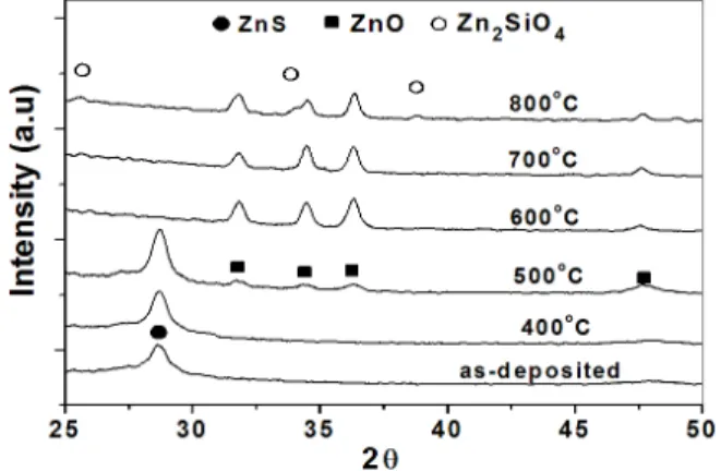
Sputter deposition of ZnO and annealing it at a high temperature is a conventional technique to create a ZnO film. In the case, it is difficult to characterize the nature of ZnO film because the composition of ZnO film can be varied in an undesirable way.

To detect the deep-level defects with green emission, the sputtered ZnO film requires an annealing temperature above 900

o

C in a H

2

atmosphere

12)

. Since the ZnO film and glass substrate react at such high temperature, the convention method of producing ZnO film cannot be applied to develop a ZnO layer on a glass substrate. Therefore, it is necessary to lower the fabrication temperature of ZnO film below 600

o

C, at which point a glass substrate can be used. If it is possible we may produce ZnO film with doping at such low temperature for

Preparation of Intrinsic ZnO Films at Low Temperature Using Oxidation of ZnS Precursor and Characterizion of the Films

Do Hyung Park

1,2)

․ Yang Hwi Cho

1,2)

․ Dong Hyeop Shin

1)

․ Byung Tae Ahn

1)

*

1)

Department of Materials Science and Engineering, Korea Advanced Institute of Science and Technology, Yuseong-gu, Daejeon, 305-701, Korea.

2)

Samsung SDI, Kiheung-gu, Yongin, 446-577, Korea

ABSTRACT: ZnO film has been used for CIGS solar cells as a buffer layer as itself or by doping Mg and Sn; ZnO film also has been used as a transparent conducting layer by doping Al or B for solar cells. Since ZnO itself is a host material for many applications it is necessary to understand the electrical and optical properties of ZnO film itself with various preparation conditions. We prepared ZnO films by converting ZnS precursor into ZnO film by thermal annealing. ZnO film was formed at low temperature as low as 500°C by annealing a ZnS precursor layer in air. In the air annealing, the electrical resistivity decreased monotonically with increasing annealing temperature;

the intensity of the green photoluminescence at 505 nm increased up to 750°C annealing. The electrical resistivity further decreased and the intensity of green emission also increased in reducing atmospheres. The results suggest that deep-level defects originated by oxygen vacancy enhanced green emission, which reduce light transmittance and enhance the recombination of electrons in conduction band and holes in valence. More oxidizing environment is necessary to obtain defect-free ZnO film for higher transparency.

Key words: Intrinsic ZnO, Low-temperature process, Resistivity, Green emission, Deep-level defect

*Corresponding author: [email protected]

Received November 29, 2013; Revised December 3, 2013;

Accepted December 9, 2013

ⓒ 2013 by Korea Photovoltaic Society

This is an Open Access article distributed under the terms of the Creative Commons Attribution Non-Commercial License (http://creativecommons.org/licenses/by-nc/3.0)

which permits unrestricted non-commercial use, distribution, and reproduction in any medium, provided the original work is properly cited.

115

(2)

many applications including buffer and electrode with substrate types.

To prepare ZnO film at low temperature, in our study, ZnS precursor was deposited on a glass substrate as a precursor layer, and then it was converted to ZnO by annealing at various temperatures and atmospheres. Prior research on growing ZnO via ZnS oxidation was done on crystalline Si at 800

o

C for near UV emission

11)

. Our work is the first attempt to grow ZnO via ZnS oxidation on a glass substrate for green emission and high conductivity. It was found that the fabrication temperature of ZnO was greatly lowered and the electrical resistivity and PL emission were well characterized and understood.

2. Experimental

ZnS precursors were deposited on a glass substrate by e-beam evaporation at a vacuum pressure of 10

-6

Torr using a ZnS pellet source. The substrate was rotated during the deposition process to improve the film uniformity and was adjusted to room temperature by a water-cooled substrate holder. The thickness of the ZnS precursor was fixed at 300 nm.

The ZnS precursors were oxidized to form ZnO film by annealing them at various temperatures for 2 h in atmospheres of air, O

2

, Ar, 4% H

2

/N

2

, and carbon. To anneal the precursors in a carbon atmosphere, the sample was surrounded by carbon powder in a closed alumina crucible. To compare our idea with the conventional method, 300 nm thick ZnO film was deposited on a glass substrate by the RF sputtering of a ZnO target and was subsequently annealed at 600

o

C for 2 h in air.

The phase and crystallographic structure were investigated by x-ray diffraction (XRD), operating at 30 kV and 60 mA using

Cu Kα (λ = 1.5405Å) radiation. The scanning range, 2θ, was from 25 to 50°. The composition of ZnO film was analyzed by Auger electron spectroscopy (AES). The optical transmission spectra were recorded with a UV-visible spectrometer in the range of 380 to 780 nm. The resistivity and sheet resistance were measured utilizing a four-point probe.

To investigate the luminescent properties, the photoluminescence (PL) was measured, using a He-Cd 325 nm laser and a photon- counting spectrometer (ISS PC1) operating at 500 W.

3. Results and Discussion

Fig. 1 shows XRD patterns of the films after annealing ZnS precursor at various temperatures for 2 h in air. The annealing temperature varied from 400 to 800

o

C with 100

o

C intervals. At 400

o

C annealing, the XRD pattern of the films shows only a ZnS sphalerite structure. The film annealed at 500

o

C shows weak ZnO peaks and strong ZnS peaks, indicating that ZnS is converting to ZnO. At 600

o

C annealing, ZnS peaks disappear, and only ZnO peaks are observed in the film. Between 500 and 700

o

C, the oxidation of ZnS takes place in the following chemical reaction

11)

.

2 ZnS + 3 O

2

= 2 ZnO + 2 SO

2

At 800

o

C annealing, the Zn

2

SiO

4

phase appears as the secondary phase in the ZnO main phase. The Zn

2

SiO

4

phase was a reaction product of the ZnO and the glass substrate with a reaction of 2 ZnO + SiO

2

= Zn

2

SiO

4

. The glass substrate is destroyed at 800

o

C by the reaction and cannot be used as a TCP substrate. With the reaction, the optical transmittance and PL

Fig. 1. XRD patterns of the films after annealing ZnS precursor at various temperatures for 2 h in air

Fig. 2. XRD patterns of the film after annealing ZnS precursor

at 500 to 525°C in air

(3)

emission of ZnO are strongly deteriorated, as will be shown later.

To find the lowest conversion temperature from ZnS to ZnO, additional annealing was performed at temperatures close to 500

o

C. Fig. 2 shows the XRD patterns of the thin films annealed at 500

o

C and 525

o

C for 2 h and 500

o

C for 12 h in air. After 2 h of annealing at 525

o

C, the ZnS precursor is completely converted to ZnO. The ZnS precursor is also completely converted to ZnO by 12 h of annealing at 500

o

C. Therefore, it can be said that the conversion temperature form ZnS to ZnO is as low as 500

o

C.

Considering that the typical high-quality ZnO film is prepared by annealing above 900

o

C after sputter deposition of ZnO film, the fabrication temperature of ZnO film using ZnS precursor is much lowered.

Fig. 3 shows the surface morphologies of the ZnO films annealed in air at (a) 500, (b) 600, (c) 700, and (d) 800

o

C. The grain size changed from 30 to 150 nm as the annealing temperature increased from 500 to 800

o

C. The surface morphology of the film was not affected by annealing atmospheres (air, O

2

, Ar, and 4% H

2

/N

2

). The thickness of ZnS precursor was 300 nm and that of ZnO was also close to 300 nm.

Fig. 4 shows (a) the AES depth profiles of Zn, O, S, and Si and (b) the AES Si depth spectra near the ZnO/Si interface after annealing at 600

o

C for 2 h in air. In Fig. 4(a), Zn and O were detected, and no S was detected in the ZnO film. The S content in the films is below the AES detection limit of 2%. However, 5~10% Si was recorded in the AES depth profile due to the noise intensity not by Si peak, as shown in Fig. 4(b). No Si peak exists in the ZnO film while a clear Si peak exists in the Si wafer region, in Fig. 4(b).

Therefore, it is thought that the 5~10% Si in the ZnO film is due to high noise intensity. We also found that the same 5~10%

Si noise exists in the ZnS precursor deposited at room temperature where Si diffusion does not occur. In our sample Si does not exist or may exist below the AES detection limit in the ZnO film.

Since we grow a ZnO film not on a Si substrate but on a glass substrate, the Si content in ZnO film is thought to be very small and the role of Si for low temperature oxidation could be negligible.

Fig. 5 shows (a) the microstructure of a ZnO film prepared by annealing a sputter-deposited ZnO film at 600

o

C for 2 h in air and (b) photoluminescence spectra of ZnO films prepared by annealing from sputter-deposited ZnO film and evaporation- deposited ZnS film by annealing at 600

o

C for 2 h in air. For the PL emission measurement, the excitation wavelength was 325 nm.

Comparing Figs. 3 and 5(a), the ZnO film fabricated from ZnS shows better-defined grain shape and more uniform grain- size distribution than the ZnO film prepared by the conventional

Fig. 3. SEM micrographs of the films after annealing ZnS precursor at 500 (a), 600 (b), 700 (c), and 800°C (d) for 2 h in air

(a)

(b)

Fig. 4. (a) AES depth profiles of Zn, O, S, and Si of the films and

(b) AES spectra near the Si peak position in the ZnO/Si

interface, after annealing ZnS precursor on Si at 600°C

for 2 h in air

(4)

method. In Fig. 5(b), a clear PL green emission was observed in the ZnO film fabricated from ZnS, while no green emission was observed in the ZnO film prepared by the conventional method.

Thus, the proposed method of fabricating ZnO film from ZnS precursor shows a major advance in lowering the fabrication temperature and obtaining a good microstructure as well as clear PL emission.

Fig. 6(a) shows the transmittance spectra of the films after annealing ZnS precursor at various temperatures. The transmittance is higher than 75% when the annealing temperature is in the range of 600 to 700

o

C. At 800

o

C annealing, the transmittance greatly decreases in the short wavelength region (400-500 nm) due to the formation of a Zn

2

SiO

4

secondary phase at the ZnO/SiO

2

interface, suggesting that annealing above 800

o

C is undesirable.

Fig. 6(b) shows the transmittance spectra of the films after annealing ZnS precursor at 700

o

C for 2 h in various atmospheres such as air, O

2

, Ar, and 4% H

2

/N

2

. The transmittance in the 450 to 500 nm region significantly decreases in reduced atmospheres.

It is thought that the defect level with a 505 nm emission peak (2.46 eV) could absorb incident photons in the short wavelength region (400-500 nm) and reduce transmittance. Note that this

absorption is not desirable for transparent electrode or buffer applications in solar cells. ZnO film should be deposited or annealed in oxygen environment for high transmittance.

Fig. 7 shows the PL spectra of the ZnO films after annealing ZnS precursor at various temperatures for 2 h in air. The film annealed at 500

o

C shows a broad emission with two apparent peaks: the first near 525 nm and the second near 450 nm. The film annealed in the range of 600 to 750

o

C shows a strong

Fig. 5. (a) Surface morphology of ZnO film annealed from sputter-deposited ZnO precursor and (b) luminescence spectra of the ZnO films fabricated from ZnS and ZnO precursors

Fig. 6. Optical transmittance spectra of the films after annealing ZnS precursor (a) at various temperatures for 2 h in air and (b) in various environments at 700°C for 2 h

Fig. 7. PL spectra of the ZnO films annealed from ZnS precursor

for 2 h in air

(5)

emission peak centered at 505 nm, while the film annealed at 800

o

C shows no peak around 505 nm and a stronger peak at 350 nm.

The peak near 525 nm arises due to the luminescence from the ZnO, and the peak near 450 nm arises due to the luminescence from the ZnS with the self-activated luminescence of oxygen impurity

7,13)

. Morozova et al. proposed that all of the self- activated bands in pure II–VI crystals are related to oxygen atom at the S lattice sites, O

S14)

. The green emission peak centered at 505 nm shown in the films annealed between 600 and 750

o

C arises due to the luminescence from ZnO with oxygen vacancies.

The green emission peak centered at 505 nm was gone when a ZnS precursor was annealed at 800

o

C due structural relaxation and the elimination of singly charged oxygen vacancies in the film. This will be discussed later.

The UV emission around 350 nm shown in Fig. 7 arises due to the free excitons in the ZnO. By increasing the annealing temperature, the intensity of the UV peak monotonically increases due to the improved crystallinity of the ZnO film. Relatively weak UV emissions compared to the 505 nm green peak are observed in all of the films. This quenching of the UV emission indicates that the crystalline ZnO samples annealed at various temperatures contain holes and/or a large number of defects that can easily trap free electrons.

Oxygen vacancies have been suggested as the main defect causing the green PL in ZnO

6,16)

. Among the three different charged states of V

O

, V

O

∙, and V

O

∙, the singly charged oxygen vacancy (V

O

∙) is thought to be responsible for the green PL emission

17)

. Since the ZnO film converted from ZnS shows a green emission, the composition of the ZnO film is considered

to be oxygen deficient.

Fig. 8 shows the electrical resistivity of the films after annealing ZnS precursor at various temperatures for 2 h in air.

The resistivity decreased from 40 to 0.02 Ω∙cm as the annealing temperature increases from 500 to 800°C. The resistivity of the films annealed at 500

o

C has a high value because the film is composed of ZnS and ZnO phases. As the annealing temperature increases, the resistivity of the ZnO film decreases monotonically.

The decrease of the resistivity at a higher temperature occurs due to the increase in the crystallinity caused by grain growth as well as the escaping tendency of oxygen at higher temperature.

As a result, the concentrations of Zn interstitials, Zn

i

, and oxygen vacancies, V

O

, can increase at higher temperature. It is known that the electrical resistivity of ZnO film decreases due to the increased concentration of singly-charged Zn interstitials

15)

.

In a comparison of Figs. 7 and 8, it is apparent that the intensity of the green PL at 505 nm increases as the electrical resistivity decreases. This is true because the oxygen vacancies increase as the annealing temperature increases. However, the PL emission peak disappears at 800

o

C while the resistivity continuously decreases. This suggests that the annealing temperature is high enough so that structural relaxation occurs in the thin film at 800

o

C. As a result, the deep-level defects caused by oxygen vacancies are removed, while the shallow-level defects caused by singly-charged Zn interstitials are maintained.

Fig. 9 shows the PL intensity of a 505 nm peak (a) and the electrical resistivity (b) of ZnO films after annealing ZnS precursor at 700°C for 2 h in air, O

2

, Ar, and 4% H

2

/N

2

. The PL intensity of ZnO film is the strongest by 4% H

2

/N

2

annealing and the weakest by O

2

annealing. The electrical resistivity is the smallest by 4% H

2

/N

2

and the largest by O

2

annealing. From the PL intensity and electrical resistivity at 700°C, it is thought that the concentrations of oxygen vacancies and Zn interstitials increase in reduced atmosphere.

In Fig. it is seen that ZnO film annealed in oxygen environment contains least oxygen vacancy and least deep-level defects. It suggests that a good deep-level defect-free ZnO film can be in oxygen environment. Even though no data is supplied here, we can infer that plasma damage by sputtering process can produce deep-level defects and deteriorate the quality of ZnO film. In that point it is preferable to prepare ZnO film by oxidizing ZnS precursor in air.

In order to see deep-level defects in ZnO more drastically, ZnS film was annealed in carbon reducing environment. Fig. 10 Fig. 8. Electrical resistivity of ZnO film, annealed at various

temperatures for 2 h in air

(6)

shows the surface morphology (a) and PL spectrum (b) of the ZnO film after annealing ZnS precursor at 700

o

C for 2 h in a carbon atmosphere. In Fig. 10(a), the grains in the ZnO film fabricated in a carbon atmosphere are well defined, and the grains size is nearly five times larger than that of the ZnO film fabricated in air.

In Fig. 10(b), the PL peak intensity of the 505 nm peak of the film annealed in a carbon atmosphere is five times stronger than that of the film annealed in air. This is attributed to the larger grain size and greater number of oxygen vacancies in the film by annealing in a strongly reduced atmosphere. It has been reported that the grain size also affects the emission intensity, where ZnO film can be applied as green phosphor layer

18,19)

.

From the results of electrical resistivity and PL luminescence of ZnO film with various environments and temperatures, it is seen that electrical resistivity continuously decreases as the annealing temperature increase (seen in Fig. 8), while the PL emission increases up to 750°C and suddenly drops at 800°C (seen in Fig. 7). This indicates that electrical resistivity is

originated from Zn interstitial; but PL emission is originated from oxygen vacancy. To avoid the optical absorption in ZnO film it is necessary to reduce the oxygen vacancy concentration in the film by supplying enough oxygen during film preparation and structural damage by sputtering also should be minimized.

4. Conclusions

In this work, ZnO film was fabricated on a glass substrate by oxidizing ZnS precursor film deposited by e-beam evaporation to understand the electrical and optical properties of intrinsic ZnO film. The ZnS film was completely converted to ZnO by annealing at temperatures as low as 500

o

C in air so that a ZnO phosphor film could be fabricated on glass substrate. Above 800

o

C annealing, a Zn

2

SiO

4

secondary phase was observed in the ZnO film by the reaction of ZnO and the glass substrate, because of which the optical transmittance and PL emission property deteriorated drastically.

The PL emission intensity of the 505 nm peak in the ZnO film (a)

(b)

Fig. 9. PL intensity at 505 nm peak (a) and electrical resistivity (b) of the ZnO films, annealed from ZnS precursor at 700°C for 2 h in various environments

(a)

(b)

Fig. 10. SEM micrograph (a) and PL spectra (b) of the ZnO films

after annealing ZnS precursor at 700°C for 2 h in a

carbon atmosphere

(7)

increased as the annealing temperature reached 750

o

C in air and then disappeared at 800

o

C annealing. On the other hand, the electrical resistivity continuously decreased with the increase of annealing temperature in air. These results suggest that the oxygen vacancy that causes PL is removed at 800

o

C by structural relaxation; the Zn interstitial that causes electrical resistivity is not. By changing the annealing atmosphere at 700

o

C, it was found that the electrical resistivity decreased and peak intensity increased in reduced atmosphere, indicating that the concentrations of oxygen vacancies and Zn interstitials increase in reduced atmosphere. The PL emission intensity of the ZnO film fabricated from ZnS at 700

o

C in a carbon atmosphere was five times stronger than that of ZnO fabricated in air. To obtain ZnO film with good transparency, it is necessary to minimize the oxygen vacancy in the ZnO film by supplying enough oxygen or avoiding damage on it.

Acknowledgments

This work was supported by the Center for Inorganic Photovoltaic Materials (No. 2012-0001167) and the Priority Research Center Program (2011-0031407), funded by the Korea Ministry of Education, Science, and Technology.

References

1. W. K. Metzger, I. L. Repins, and M. A. Contreras, “Long life- times in high-efficiency Cu(In, Ga)Se

2

solar cells”, Appl. Phys.

Lett., 93, 022110 (2008).

2. C.S. Lee, L. Larina, Y. M. Shin, E.A. Al-Ammar, and B. T.

Ahn, “Design of energy band alignment at the ZnMgO/Cu(In, Ga)Se

2

interface for Cd-free Cu(In, Ga)Se

2

solar cells’, Phys.

Chem. Chem. Phys. M 14, 4789-4795 (2012).

3. C. S. Lee, K. H. Yoon, and B. T. Ahn, “Improved optical trans- mittance of boron doped ZnO thin film by low pressure chem- ical vapor deposition with pulse boron doping”, J. Electrochem.

Soc., 158, H482-H486 (2011).

4. J.F. Muth, R.M. Kolbas, A.K. Sharma, and S. Oktyabrsky,

“Excitonic structure and absorption coefficient measurements of ZnO single crystal epitaxial films deposited by pulsed laser deposition”, J. Appl. Phys. 85, 7884-7887 (1999).

5. D. H. Park, Y. H. Cho, Y. R. Do, and B. T. Ahn,

“Characterization of Eu-doped SnO

2

thin films deposited by ra- dio-frequency sputtering for a transparent conductive phosphor layer”, J. Electrochem. Soc., 154, H63-H67 (2006).

6. K. Vanheusden, C. H. Seager, W. L. Warren, D. R. Tallant, and J. A. Voigt, “Correlation between photoluminescence and oxygen vacancies in ZnO phosphors”, Appl. Phys. Lett. 68, 403-405 (1996).

7. R. M. Nyffenegger, B. Craft, and R. M. Penner, “A hybrid elec- trochemical/chemical synthesis of zinc oxide nanoparticles and optically intrinsic thin films”, Chemistry of Materials 10, 1120-1129 (1998).

8. K. Iwata, P. Fons, S. Niki, A. Yamada, K. Matsubara, K.

Nakahara, T. Tanabe, and H. Takasu, “ZnO growth on Si by radical source MBE”, J. Crystal Growth 214, 50-54 (2000).

9. R.D. Vispute, Y.X. Li, A.A. Iliadis, and K.A. Jones, “Heteroepitaxy of ZnO on GaN and its implications for fabrication of hybrid optoelectronic devices”, Appl. Phys. Lett. 73, 348-350 (1998).

10. E.M. Wong, and P.C. Searson, “ZnO quantum particle thin films fabricated by electrophoretic deposition”, Appl. Phys.

Lett. 74, 2939-2941 (1999).

11. A. Miyake, H. Kominami and Y. Hatanaka, “Growth of epi- taxial ZnO thin film by oxidation of epitaxial ZnS film on Si(111) substrate”, Jpn. J. Appl. Phys. 39, L1186-L1187 (2000).

12. M. Liu, A. H. Kitai, and P. Mascher, “Point defects and lumi- nescence centers in zinc oxide doped with manganese”, J.

Lumin., 54, 35-42 (1992).

13. T. Igarashi, T. Kusunoki, K. Ohno, T. Isobe,and M. Senna,

“Degradation proof modification of ZnS-based phosphors with ZnO nanoparticles”, Mater. Res. Bull. 36, 1317-1324 (2001).

14. N. K. Morozova, I. A. Karetnikov, V. V. Blinov, and E. M.

Gavrishchuk, “A study of luminescence centers related to cop- per and oxygen in ZnSe”, Semiconductors, 35, 24-32 (2001).

15. M. W. Barsoum, Fundamentals of Ceramics, p. 208, Institute of Physics, Bristol (2003).

16. P. Yang, M. Lu, D. Xu, D.L. Yuan, and G.J. Zhou,

“Photoluminescence properties of ZnS nanoparticles co-doped with Pb

2+

and Cu

2+

”, Chem. Phys. Lett. 336, 76-80 (2001).

17. S. W. Lee, D. Kim, H. J. Won, and W. Y. Chung, “Electrical Conductivity and Defect Structure of CeO

2

-ZnO System”, Electron. Matter. Lett. 2, 53-58 (2006).

18. Y. H. Cho, D. H. Park, and B. T. Ahn, “Low-temperature syn- thesis of Eu-doped cubic phase BaAl

2

S

4

blue phosphor using liquid-phase reaction”, J. Electrochem. Soc., 155, J41-J44 (2008).

19. Y. H. Cho, R. B. V. Chalapathy, CD. H. Park, and B. T. Ahn,

“Low-temperature synthesis of Eu-doped cubic phase BaAl

2

S

4

blue phosphor using H

3

BO

3

and B

2

O

3

”, J. Electrochem. Soc.,

157, J45-J49 (2010).

수치

Fig. 1. XRD patterns of the films after annealing ZnS precursor  at various temperatures for 2 h in air
Fig. 3 shows the surface morphologies of the ZnO films  annealed in air at (a) 500, (b) 600, (c) 700, and (d) 800 o C
Fig. 5. (a) Surface morphology of ZnO film annealed from  sputter-deposited ZnO precursor and (b) luminescence  spectra of the ZnO films fabricated from ZnS and ZnO  precursors
Fig. 8 shows the electrical resistivity of the films after  annealing ZnS precursor at various temperatures for 2 h in air
+2

참조

관련 문서

Methods: Growth characteristic and opti- cal properties of the amorphous or nano-crystalline ZnO thin films prepared on soda – lime – silica glass sub- strates by chemical

We found that the post deposition annealing under oxidizing ambient causes the oxidation of residual Hf metal components, resulting in the improvement

However, due to the limitation of the requirement of a very high deposition temperature along with post annealing and a low growth rate, extensive research are being undertaken