Vol. 13, No. 3, pp. 73-77, September 2008
Preparation of ZnO Thin Films with UV Emission by Spin Coating and Low-temperature Heat-treatment
Bo-An Kang and Ju-Hyun Jeong*
Department of Biomedical Engineering, Nambu University, Republic of Korea
*Department of Ophthalmic Optics, Konyang University, Republic of Korea (Received July 12, 2008: Revised August 6, 2008: Accepted September 10, 2008)
···
Purpose: This research is that prepare amorphous or crystalline ZnO thin films with pure strong UV emission on soda-lime-silica glass (SLSG) substrates by low-temperature annealing. Methods: Growth characteristic and opti- cal properties of the amorphous or nano-crystalline ZnO thin films prepared on soda – lime – silica glass sub- strates by chemical solution deposition at 100, 150, 200, 250 and 300°C were investigated using X-ray diffraction analysis, ultraviolet – visible – near infrared spectrophotometer, and photoluminescence. Results: The films exhibited an amorphous pattern even when finally annealed at 100°C~200°C for 60 min, while crystalline ZnO was obtained by prefiring at 250 and 300°C. The photoluminescence spectrum of amorphous ZnO films shows a strong NBE emission, while the visible emission is nearly quenched. Conclusions: These results indicate it should be possible to cheaply and easily fabricate ZnO-based optoelectronic devices at low temperature, below 200°C, in the future.
Key words: ZnO thin film, Chemical solution deposition, Photoluminescence spectrum
···
Introduction
Zinc oxide based coatings are of much interest in sci- ence and technology due to their interesting potential applications
1-3, such as in thermoelectric and gas sensor devices, transparent electrodes, selective surfaces, piezo- electric devices, etc. The wide range of applications is a result of the fact that ZnO is both a piezo-electric and electro-optic (EO) materials, and a semiconductor which possesses a wide band gap (3.3 eV)
4. The most unique property of ZnO is its large exciton binding energy of 60 meV, which is much larger than those of GaN (24 meV), ZnSe (19 meV) and ZnS (39 meV)
5. Because of this large binding energy, the exciton is stable at room tem- perature even in bulk crystals. Owing to these properties, ZnO is considered as a promising material for light-emit- ting devices and semiconductor lasers with low thresholds in the ultraviolet (UV) region. Generally, the correspond- ing photoluminescence (PL) spectra obtained from ZnO
thin films shows defect-related deep-level emission
6,7(yellow-green emission around 510 nm and red emission around 650 nm) as well as UV near-band-edge emission around 380 nm, which strongly depends upon the prepa- ration methods and growth conditions.
Using molecular beam epitaxy (MBE), rf magnetron sputtering, metal organic chemical vapor deposition (MOCVD) and other methods, high quality ZnO layers have been grown and their structural and optical proper- ties have been extensively studied
8-11. However, most of the reports on the UV emission of ZnO films have been concentrated on high-vacuum processes which are very expensive method from the viewpoint of system and source materials. To meet the industrial needs for the commercially available ZnO devices, the easier and cheaper deposition methods for the ZnO film should be developed. Chemical solution deposition (CSD) is another attractive technique for obtaining thin films and has the advantages of easy control of the film composition and
Corresponding Author Address: Ju-Hyun Jeong, 685 Gasuwon-dong, Seo-gu, Daejeon 302-718, Korea TEL: +82-42-600-6333, E-mail: [email protected]
easy fabrication of a large-area thin film at low cost
12-15. Only a few researchers reported that there was accompa- nied single violet emission of ZnO prepared by CSD
16.
In this work, we first report a simple and efficient method to prepare amorphous or crystalline ZnO thin films with pure strong UV emission on soda-lime-silica glass (SLSG) substrates by low-temperature annealing.
Methods
A homogeneous coating solution was prepared by mix- ing Zn acetate [(CH
3COO)
2Zn·2H
2O] (Merck,Germany) and 2-methoxyethanol (HOCH
2CH
2OCH
3) (Merck, Ger- many). Since Zn acetate has alow solubility in 2-methoxy ethanol, 2-aminoethanol (H
2NCH
2CH
2OH) (MEA) (Merck, Germany) was added to obtain clear solution (concentra- tion: 0.6 mol Zn acetate/L2-methoxyethanol). The molar ratio of MEA to Zn acetate was fixed at 1.0. The mixing solution was stirred for 2 h to obtain a homogeneous pre- cursor solution.
Prior to coating process, SLSG substrates were cleaned in deionized water, immersed in H
2O
2solution, and finally rinsed in acetone. The starting solution was spin- coated onto the cleaned substrate at 4000 rpm for 10 sec in air. The as-deposited film was prefired at 100
oC, 150
oC, 200
oC, 250
oC and 300°C for 10 min in air. The coating process was repeated 13 times to prepare a thick coating of ZnO. Then the final annealing was performed in air at 100
oC, 150
oC, 200
oC, 250
oC and 300°C for 60 min.
The thickness of the finally annealed ZnO thin film was approximately 0.5~0.7 µm, as determined by F20 (Filmetric Inc., San Diego, U.S.A.) using reflection spec- trum and the observation of fracture cross-section with a field emission – scanning electron microscope (FE-SEM, S-4700, Hitachi, Japan). Thermogravimetric analysis (TGA, DTG-60, Shimadzu, Japan) of the precursor solution was performed (heating rate: 2°C/min, in air). The crystallinity of the ZnO thin films was investigated by using a high resolution X-ray diffraction (HRXRD, X’pert-PRO, Phil- ips, Netherlands). A CuKα (λ = 1.54056 Å) source was used, and the scanning range was between 2θ=20° and 70°. The transmittance in the visible range was measured using UV – visible – NIR spectrophotometer (CARY 500 Scan, Varian, Australia). The transmittance was automati-
cally calibrated against that of a bare SLSG substrate as a reference sample, and the absorption coefficient was obtained from the transmittance curve. Room temperature photoluminescence (PL) spectra of the samples were measured by micro-PL system (LabRamHR, Jobin Yvon, France) using 325 nm line of a He-Cd laser as the exci- tation source.
Results and Discussion
Fig. 1 shows TGA curve of the precursor solution used in this work. A larger weight loss corresponding to pyrol- ysis of the precursor solution began around 130°C and was completed just below about 200°C, as shown in Fig.
1. TGA curve of the precursor solution (heating rate:
2°C/min) showed large weight loss due to the vaporiza- tion and pyrolysis of organics were recognized in the stage of pyrolysis at 150~200°C. Therefore, pyrolysis of the precursor solution is completed below about 200°C.
Thus, to investigate the effects of temperatures during prefiring and final annealing, we prepared ZnO films via the above-mentioned prefiring and annealing conditions in our experimental procedure.
Fig. 1. TGA curve of the precursor solution used in this work.
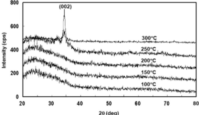
Fig. 2. HRXRD spectra of the ZnO thin films on SLSG
substrates heat treated at various temperatures.
Fig. 2 shows the XRD curves of ZnO thin films depos- ited on SLSG substrates. A (002) peak with a weak (100) reflection is observed at 2θ=34° for the samples heat treated at 250 and 300°C. The films show an amorphous pattern even when finally annealed at 100~200°C for 60 min, which implies the most of the processes occurring up to 200°C are mainly related to removal of organic compounds in precursor, as shown in Fig. 1. On the basis of the XRD data, the lattice c parameter has been esti- mated to be 5.2284 and 5.2700 Å at 250 and 300°C, respectively. This value is similar to the ASTM value of 5.2066 Å for the bulk ZnO. The larger value of lattice constant for the film at 250 and 300°C compared to the standard powder value shows that unit cell is elongated along the c-axis, and that compressive forces act in the plane of the ZnO film.
UV transmission measurements were carried out for optical characterization of the films. Fig. 3 shows the vis- ible spectra in the wavelength range from 300 nm to 900 nm of the ZnO thin films annealed at various tempera- tures on SLSG substrates. A relatively high transmittance above 80% in the visible spectra range and clear absorp- tion edges of the films were observed except the film annealed at 100°C. The transmittance in the UV spectra region decreased abruptly near 3.2~3.3 eV, resulting from band – to – band transition. In this transition, UV absorp- tion occurs due to the excitation of electrons from the filled valence band to the conduction band. The slopes of the absorption edge are sharpened and there is an obvious shift of the absorption edge to longer wavelength with increasing processing temperature.
The optical absorption coefficient a of the films can be
calculated from the transmittance using the relationship,
I = I
0e
−αt(1)
where I is the intensity of transmitted light, I
0is the inten- sity of the incident light, and t is the thickness of the ZnO film. As the transmittance is defined as I/I
0, we obtain a from Eq. (1). It is well known that the absorption coeffi- cient a for allowed direct transitions at a given photon energy hn can be expressed as,
α = (hν−Eg)
1/2(2)
where, h is Plank’s constant, ν is the frequency of the incident photon, and Eg is optical energy band gap of the film. By plotting α
2versus hν and extrapolation the linear position of the curves to plotting α
2is zero is Eg. The estimated values of the band gap for the ZnO films annealed at various temperatures by an extrapolation method
17are 3.41 eV, 3.34 eV, and 3.30 eV at 150°C, 200°C, and 250°C, respectively, close to the intrinsic band gap of ZnO (3.2 eV). As can be seen clearly, Eg values decrease from 3.41 eV to 3.30 eV with an increase of heating temperature. In other words, the optical energy band gap of our films becomes shorter as heating temper- ature increases.
The PL spectra at room temperature of amorphous or nano-crystalline ZnO thin films on SLSG substrates obtained by pyrolysis and annealing at 100°C, 150°C, 200°C, 250°C and 300°C is shown in Fig. 4. In the PL spectra, only a strong near-band-edge (NBE) emission is seen for all films except film annealed at 150°C. This NBE peak has been previously attributed to the emission from free exciton in the literature
18. After annealing at
Fig. 3. UV-visible spectra of the ZnO thin films on SLSG substrates heat treated at various temperatures.
Fig. 4. The PL spectra at room temperature for the ZnO thin
films on SLSG substrates heat treated at various
temperatures.
250
oC and 300°C, the PL spectra of the film was slightly deteriorated, the UV peak was diminished. M. Choi et al.
19reported that the non-radiactive recombination cen- tres were generated by the oxygen vacancies, which increase with increasing temperature. For the film anneal- ed at 200°C, the largest NBE peak intensity in the PL spectra was observed. This indicates that the annealing temperature of 200°C is an optimum condition for the formation of ZnO thin film with a strong single NBE emission. A distinct defect-related broad green (deep- level) emission is not seen in all the samples except the film annealed at 150°C. The origin of the green lumines- cence is still in dispute, but it is usually attributed to emission related to grain boundary defects and other inte- rior defects such as oxygen vacancy (VO) and impurities
20. Apparently, for the film annealed at low temperature, 200°C, the FWHM value of the PL spectrum curve was 28.7 meV and this value is believed to be comparable with any previously reported values of ZnO films pre- pared by chemical solution deposition.
The PL spectrum of amorphous ZnO thin films with strong UV emission was observed while the visible emis- sion was nearly fully quenched. The features can be explained reasonably by Z. Wang et al. as follows
16: (i) The higher degree of disorder likely leads to intensity emission stronger than that of crystalline ZnO. (ii) Quan- tum confinement effects (QCE) occur when the particle radius is of the order the exciton Bohr radius (1.8 nm, ZnO). Although it is difficult to obtain the exact diameter of amorphous ZnO, we assume that the sizes of amor- phous ZnO are smaller than 1.8 nm.
It is well understood that PL spectra depend on the sto- ichiometry and the microstructure of the film. Therefore, these results indicate that the obtained amorphous ZnO films at low temperature are well close to stoichiometry and of optically high quality. Our findings show that the PL property of the ZnO thin films is improved because the grain size decreases with low-temperature annealing.
Conclusions
In this study, amorphous or nano crystalline ZnO thin films were grown on inexpensive SLSG substrates using chemical solution deposition with a zinc acetate − 2 meth- oxy ethanol – MEA solution. From XRD analysis, the
films exhibited an amorphous pattern even when finally annealed at 100°C~200°C for 60 min, while crystalline ZnO was obtained by prefiring at 250 and 300°C. A rel- atively high transmittance in the visible spectra range and clear absorption edges of the films were observed except the film annealed at 100°C. From the PL measurement, a strong NBE emission was observed for the ZnO film annealed at 200°C, while the deep-level emission is almost undetectable except the film annealed at 150°C.
These results indicate it should be possible to cheaply and easily fabricate ZnO-based optoelectronic devices at low temperature, below 200°C, in the future.
Acknowledgements
This study was supported by a grant of the Korea San- hak Foundation (2007), Republic of Korea.
References
1. Hwang S. K., Jeon Y. S, Kang B. A., An J. H., and Kim B.
H., “Nanocrystalline ZnO films on amorphous substrates from zinc naphthenate”, J. Ceram. Proc. Res., 5(4):313- 315(2004).
2. Kim B. H., An J. H., Jeon Y. S., Jeong J. T., Kang B. A., and Hwang K. S., “Highly c-axis oriented ZnO film on sil- ica glass using zinc naphthenate precursor”, J. Mater. Sci., 40(1):237-239(2005).
3. Bian J., Li X., Chen L., and Yao Q., “Properties of undoped n-type ZnO film and N-. In codoped p-typeZnO film deposited by ultrasonic spray pyrolysis”, Chem. Phys.
Lett. 393:256-259(2004).
4. Webb J. B., Williams D. F., and Buchanan M., “Transpar- ent and Highly Conductive Films of ZnO Prepared by RF Reactive Magnetron Sputtering”, Appl. Phys. Lett., 39:
640-642(1981).
5. Chen Y. F., Bagnall D. M., Hoh H. J., Park K. T., Hiraga K., Zhu Z., and Yao T., “Plasma assisted molecular beam epitaxy of ZnO on c-plane sapphire: Growth and character- ization”, J. Appl. Phys., 84(7):3912-3918(1998).
6. Zhao B., Yang H., Du G., Fang X., Liu D., Gao C., Liu X., and Xie B., “Preparation and optimization of ZnO films on single-crystal diamond substrate by metal-organic chemical vapour deposition”, Semicond. Sci. Technol. 19:770-773 (2004).
7. Kim I. S., Jeong S. H., Kim S. S., and Lee B. T., “Magne- tron sputtering growth and characterization of high quality single crystal ZnO thin films on sapphire substrates”, Semicond. Sci. Technol., 19:L29-L31(2004).
8. Tampo H., Yamada A., Fons P., Shibata H., Matsubara K.,
Iwata K., Niki S., Nakahara K., and Takasu H., “Degener- ate layers in epitaxial ZnO films grown on sapphire sub- strates”, Appl. Phys. Lett. 84(22):4412-4414(2004).
9. Kim K. K., Song J. H., Jung H. J., Park S. J., Song J. H., and Lee J. Y., “Photoluminescence and heteroepitaxy of ZnO on sapphire substrate (0001) grown by rf magnetron sputtering”, J. Vac. Sci. Technol A., 18(6):2864-2868(2000).
10. Park W. I., An S. J., Yi G. C., and Jang H. M., “Metal- organic vapor phase epitaxial growth of high-quality ZnO films on Al
2O
3”, J. Mater. Res., 16(5):1358-1362(2001).
11. Wang L., Pu Y, Fang W., Dai J., Zheng C., Mo C., Xiong C., and Jiang F., "Effect of high-temperature annealing on the structural and optical properties of ZnO films”, Thin Solid Films, 491:323-327(2005).
12. Natsume Y. and Sakata H., “Zinc Oxide Films Prepared by Sol-Gel Spin-Coating”, Thin Solid Films, 372:30-36(2000).
13. Ayouchi R., Leinen D., Martin F., Gabas M., Dalchiele E., and Ramos-Barrado J. R., “Preparation and characteriza- tion of transparent ZnO thin films obtained by spray pyrol- ysis”, Thin Solid Films, 426:68-77(2003).
14. Nunes P., Fortunato E., and Martins R., “Influence of the post treatment on the properties of ZnO thin films”, Thin Solid Films, 383:277-280(2001).
15. Paraguay F. D., Morales J., Estrada W. L., Andrade E., and
Miki-Yoshida M., “Influence of Al, In, Cu, Fe and Sn dopants in the microstructure of zinc oxide thin films obtained by spray pyrolysis”, Thin Solid Films, 366:16- 27(2000).
16. Wang Z., Zhang H., Wang Z., Zhang L., Yuan J., Yan S., and Wang C., “Structure and strong ultraviolet emission characteristics of amorphous ZnO films grown by electro- phoretic deposition”, J. Mater. Res., 18(1):151-155(2003).
17. Shimono D., Tanaka S., Torikai T., Watari T., and Murano M., “Preparation of transparent and conductive ZnO films using a chemical solution deposition process”, J. Ceram.
Proc. Res., 2(4):184-188(2001).
18. Park W. I. and Yi G. C., “Photoluminescent properties of ZnO thin films grown on SiO
2/Si(100) by metal-organic chemical vapor deposition”, J. Electron. Mater., 30:L32- L35(2001).
19. Choi M. H. and Ma T. Y., “Influence of substrate tempera- ture on ultraviolet emission of ZnO films prepared by ultra- sonic spray pyrolysis”, J. Mater. Sci., 41:431-435(2006).
20. Look D. C., Reynolds D. C., Sizelove J. R., Jones R. L., Litton C. W., Cantwell G., and Harsch W. C., “The wafers of ZnO used in this research were grown via the seeded vapor-phase technique”, Sold State Commun., 105(6):399- 401(1998).
스핀코팅 및 저온열처리에 의한 자외선 발광특성을 갖는 산화아연 박막의 제조