1. 서 론
IGBT (insulated gate bipolar transistor) 소자는 전류전도 능력이 뛰어난 소자이며, 큰 전력을 처리하기 위해 설계된 스위칭 디바이스로서 전원 공급 장치, 변 환기, 태양광 인버터, 가전제품 등에 널리 사용되고 있 다. 이러한 IGBT는 파워 반도체 소자인 만큼 항복 전
a. Corresponding author; [email protected] Copyright ©2017 KIEEME. All rights reserved.
This is an Open-Access article distributed under the terms of the Creative Commons Attribution Non-Commercial License (http://creativecommons.org/licenses/by-nc/3.0) which permits unrestricted non-commercial use, distribution, and reproduction in any medium, provided the original work is properly cited.
압과 온상태 전압 강하, 스위칭 속도, 신뢰성의 이상적 인 파워 반도체 소자의 요구사항을 목표로 하고 있다.
일반적으로 드리프트 영역의 농도를 낮추게 되면 항복 전압은 증가하지만 온 저항과 같은 기타 특성들이 감 소하게 되므로 설계의 최적화 및 구조 변경을 통해 항 복전압특성과 온 상태 전압강하 특성을 개선 시켜야 한다. 이렇듯 IGBT 소자의 효율을 높이기 위해 트레이 드-오프 관계를 최적화시키고자 여러 가지 구조들이 나 오고 있다. 본 논문에서는 공정 시뮬레이터인 T-CAD를 사용하여 NPT-IGBT (non punch through- IGBT) 그 리고 필드 스톱 IGBT (field stop-IGBT)의 전기적인 특성을 분석하였다.
고전압 Non Punch Through IGBT 및 Field Stop IGBT 최적화 설계에 관한 연구
강이구
a
극동대학교 태양광공학과
The Optimal Design of High Voltage Non Punch Through IGBT and Field Stop IGBT
Ey Goo Kang a
Department of Photovoltaic Engineering, Far East University, Eumseong 27601, Korea (Received January 23, 2017; Revised February 22, 2017; Accepted February 23, 2017)
Abstract: An IGBT (insulated gate bipolar transistor) device has an excellent current-conducting capability. It has
been widely employed as a switching device to use in power supplies, converters, solar inverters, and household appliances or the like, designed to handle high power. The aim with IGBT is to meet the requirements for use in ideal power semiconductor devices with a high breakdown voltage, an on-state voltage drop, a high switching speed, and high reliability for power-device applications. In general, the concentration of the drift region decreases when the breakdown voltage increases, but the on-resistance and other characteristics should be reduced to improve the breakdown voltage and on-state voltage drop characteristics by optimizing the design and structure changes. In this paper, using the T-CAD, we designed the NPT-IGBT (non punch-through IGBT) and FS-IGBT (field stop IGBT) and analyzed the electrical characteristics of those devices. Our analysis of the electrical characteristics showed that the FS-IGBT was superior to the NPT-IGBT in terms of the on-state voltage drop.Keywords: IGBT, Non punch through, Filed stop, Breakdown voltage, On state voltage drop
Regular Paper
214J. Korean Inst. Electr. Electron. Mater. Eng.
Vol. 30, No. 4, pp. 214-217 April 2017
DOI: https://doi.org/10.4313/JKEM.2017.30.4.214
ISSN 1226-7945(Print), 2288-3258(Online)
전기전자재료학회논문지, 제30권 제4호 pp. 214-217, 2017년 4월: 강이구 215
2. 실험 방법
본 논문에서 제시하는 NPT 및 field stop IGBT의 최적 설계를 위해서 TCAD를 이용하여 공정시뮬레이션 을 수행하였으며, 이를 통하여 최적 구조를 구현하였 다. 그리고 최적 구조를 이용하여 소자 시뮬레이션을 수행하여 소자들의 전기적인 특성을 분석하였다.
3. 결과 및 고찰
3.1 Non punch through IGBT 설계 및 전기적 특성분석
NPT (non punch through) IGBT를 설계하기 위해 항복전압을 30% 마진율을 고려하여 1,800 V를 목표로 설계를 진행함과 동시에 에피저항을 50∼75 Ω로 변화 시키면서 시뮬레이션을 실행하여 1,800 V에 최대한 가 까운 1,802.77 V를 얻을 수 있었다. 문턱전압은 4 V 로 설정하였으며, vce-sat의 값을 구하기 위해 P-base의 값을 조절하여 문턱전압을 4.213 V를 구한 후 vce-sat의 값으로 5.14 V를 도출할 수 있었다. 그 림 2는 NPT IGBT의 항복전압 특성을 보여주고 있으 며, 그림 3은 P 베이스의 농도에 따른 문턱전압과 온 전압 강하 특성을 보여주고 있다. 이러한 전기적인 특 성을 분석한 후 최적의 P 베이스 농도를 설정한 후 그 림 4와 5에서는 문턱전압과 온상태 전압강하 특성을 보여주고 있다.
Classification Size Gate (N.poly) 1.25 μm
Pitch 6.5 μm P-base dose 6×10 13 cm -2 N+ Emitter width 1 μm
Gate oxide 950 Å Total depth 320 μm N-Epi resist 63.5 Ω N-Epi depth 319.5 μm
Fig. 1. The structure and parameters of planar gate type NPT- IGBT parameter.
Fig. 2. The breakdown voltage characteristics of 1,800 V non punch through IGBT.
Fig. 3. The threshold and on state voltage drop characteristics of NPT IGBT according to P–base dose.
Fig. 4. The threshold voltage characteristics of NPT IGBT.
216 J. Korean Inst. Electr. Electron. Mater. Eng., Vol. 30, No. 4, pp. 214-217, April 2017: E.-G. Kang
3.2 Field stop IGBT 설계 및 전기적인 특성 분석
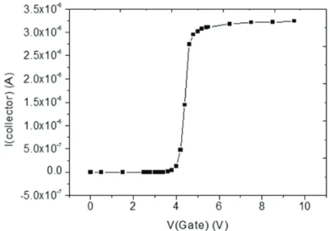
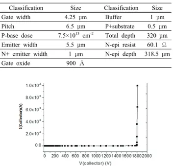
필드 스톱 IGBT를 설계하기 위해 NPT IGBT와 마찬 가지로 항복전압의 전력손실율 20%를 생각하여 1,800 V로 선택하였으며, 에피저항을 58∼62 Ω까지 변화시 키면서 시뮬레이션을 수행하였다. 1,800 V에 가장 근 접한 에피 저항은 60.1 Ω이지만 문턱전압이 4 V 미 만이기에 에피저항이 60.5 Ω이면서 동시에 항복전압 이 1,810 V인 값으로 설정하였다. 또한 표 1을 바탕으 로 제작한 필드스톱 IGBT의 P-base dose에 변화를 주어 그림 9와 같이 Vth가 4 V 이상으로 도출되는 P-base dose를 참고하여 설계를 수행하였다. 그림 7 은 필드스톱 IGBT의 항복전압 특성을 보여주고 있으 며, 그림 8은 에피 저항의 변화에 따른 항복전압과 온
Fig. 5. The on state voltage drop characteristics of NPT IGBT.
Fig. 6. The structure of planar gate type field stop IGBT.
Classification Size Classification Size
Gate width 4.25 μm Buffer 1 μm
Pitch 6.5 μm P+substrate 0.5 μm
P-base dose 7.5×10 13 cm -2 Total depth 320 μm Emitter width 5.5 μm N-epi resist 60.1 Ω N+ emitter width 1 μm N-epi depth 318.5 μm
Gate oxide 900 Å
Table 1. The parameters of planar gate type field stop IGBT.
Fig. 7. The breakdown voltage characteristics of field stop IGBT.
Fig. 8. The breakdown and on state voltage drop characteristics of field stop IGBT according to epi resist.
Fig. 9. The threshold voltage characteristics of field stop IGBT
according to P base dose.
전기전자재료학회논문지, 제30권 제4호 pp. 214-217, 2017년 4월: 강이구 217
상태 전압 강하 특성을 보여주고 있다. 그림 9는 최적 의 문턱전압을 얻기 위해 P 베이스 농도에 따른 문턱 전압과 온상태 전압강하 특성을 보여주고 있다.
표 2에서는 앞서 수행하였던 NPT IGBT와 필드스톱 IGBT 소자의 전기적인 특성들에 대해서 비교분석하였 다. 비교분석한 결과 필드스톱 IGBT가 비슷한 항복전압 을 유지하면서 작은 온 상태 전압 값을 갖고 있어 그만 큼 전력 손실이 줄어 들 수 있다는 것을 알 수 있었다.
4. 결 론
본 논문에서는 N형 웨이퍼에 planar type으로 쌓고 아랫면에 P형 collecter를 쌓은 형태인 1,500 V급 NPT IGBT 그리고 NPT IGBT와 설계 과정은 비슷하지 만 collecter를 쌓기 전에 N+를 삽입하여 버퍼를 생성 한 후 P형 collecter를 쌓은 필드스톱 IGBT를 설계하였 다. 설계한 후 전기적인 특성을 도출하였으며, 동시에 두 소자에 대해서 문턱전압, 온 상태전압 강하 그리고 항복전압에 대해서 비교 분석하였다. 비교한 결과 필드
스톱 IGBT 소자가 N+ 버퍼층으로 인하여 드리프트 층 에서 전계가 일정하게 유지되어 NPT 소자의 항복전압 을 유지하면서 작은 온 저항을 갖는 다는 것을 알 수 있었다. 따라서 향후, 1,700 V 이상의 고전압에 대해서 스위칭 소자로 큰 역할을 할 수 있을 것으로 판단된다.
REFERENCES