DOI: http://dx.doi.org/10.4313/JKEM.2012.25.4.261
600 V급 Planar Field Stop IGBT 최적 설계 및 전기적 특성 분석에 관한 연구
남태진1, 정은식2, 강이구1,a
1 극동대학교 태양광공학과
2 메이플 세미컨덕터(주)
A Study on Optimal Design and Electrical Characteristics of 600 V Planar Field Stop IGBT
Tae-Jin Nam1, Eun-Sik Jung2, and Ey-Goo Kang1,a
1 Department of Photovoltaic Engineering, Far East University, Chungbuk 369-700, Korea
2 Maple Semiconductor, Incorporated Bucheon 421-150, Korea
(Received March 20, 2012; Revised March 24, 2012; Accepted March 24, 2012)
Abstract: IGBT(insulated gate bipolar transistor) is outstanding device for current conduction capabilities.
IGBT design to control the large power switching device for power supply, converter, solar converter, electric home appliances, etc. like this IGBT device can be used in many places so to increase the efficiency of the various structures are coming. in this paper optimization design of planar type IGBT and planar field stop IGBT, and both devices have a comparative analysis and reflection of the electrical characteristics.
Keywords: Field stop, IGBT, Non-punch through, Power device
1. 서 론1)
IGBT (insulated gate bipolar transistor) 소자는 전류전도 능력이 뛰어난 소자이며, 큰 전력을 처리하 기 위해 설계된 스위칭 디바이스로써 전원 공급 장 치, 변환기, 태양광인버터, 가전제품 등에 널리 사용 되고 있다. 이러한 IGBT는 파워 반도체 소자인 만큼 항복 전압과 온-상태 전압 강하, 스위칭 속도, 신뢰성 의 이상적인 파워 반도체 소자의 요구사항을 목표로 하고 있다. 일반적으로 드리프트 영역의 농도를 낮추 게 되면 항복 전압은 증가하지만 온 저항과 같은 기 타 특성들이 감소하게 되므로 설계의 최적화 및 구조 변경을 통해 항복전압특성과 온 상태 전압강하 특성 a. Corresponding author; [email protected]
을 개선시켜야 한다. 이렇듯 IGBT 소자의 효율을 높 이기 위해 tread-off 관계를 최적화 시키고자 여러 가 지 구조들이 나오고 있다. 본 논문에서는 같은 항복전압 을 가지면서 온 상태 전압강하를 낮출 수 있는 field stop 구조를 가지는 IGBT를 제안하고 최적화된 non-punch through planar IGBT와 field stop IGBT를 설계하여 두 소자의 전기적 특성을 비교 분석 및 고찰하였다.
2. 실험 방법 2.1 Field stop 구조의 특징
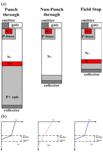
IGBT의 종류인 punch through와 Non-punch through
(a)
(b)
Fig. 1. Punch through, nun-punch through, field stop (a) basic structure, (b) electric field.
그리고 field stop의 전계 분포도를 그림 1에 나타냈 다. 그림에서 보듯 cell pitch가 동일한 상태 에서 PT 가 NPT보다 전계의 넓이는 넓지만 길이가 많이 길 다. NPT와 FS를 비교해보면 FS가 PT와 비슷한 넓 이를 가지고 있으며 길이도 가장 짧은 것을 확인할 수 있다.
그림 2는 IGBT의 온 상태 전항을 나타낸 그림이 다. 그림에서 가장 크게 온 상태 전압 강하에 영향을 미치는 저항은 RJ와 RD가 가장 많은 저항 부분을 차 지한다. 이 저항들은 수식 (1), 수식 (2)에서 보듯 n-drift영역의 저항률과 관계된 저항이며 이 저항률은 n-dritf의 농도와 길이에 의해 정해진다.
(1)
Fig. 2. IGBT on-resistance.
(2)N-drift의 농도 조절 및 field stop 구조를 사용하여 N-drift의 길이를 줄임으로써 같은 크기의 cell pitch 를 사용하는 NPT IGBT보다 높은 항복전압과 낮은 온 상태 전압강하를 구현할 것이다.
2.2 600 V급 planar type IGBT 설계
NPT planar IGBT와 field stop IGBT를 비교하기 위해 cell depth와 N buffer, N drift resistivity을 제 외한 나머지 모든 parameter들을 동일시하는 조건으 로 각각의 소자를 설계하였다. 그림 3에서 NPT planar IGBT 구조와 최적 parameter를 나타내었고 이를 시뮬레이션으로 구연하였다. 또한 동일한 600 V 급 NPT planar IGBT 구조에 N buffer층을 넣은 field stop IGBT도 설계하였다. 이를 그림 3과 그림 4 에 도시하고 그 design parameter를 표시하였다.
N-drift 비저항은 NPT planar IGBT의 최적값은 30 Ω㎝이며 field stop planar IGBT의 최적값은 40 Ω㎝
이였다. 또한 모든 IGBT의 문턱전압을 약 4.0 V로 동일하게 P-base dose량을 조절하였다. N buffer층 형성을 위한 back implantation을 실험하였다.
이와 같이 설계된 NPN planar IGBT와 field stop planar IGBT의 중요한 전기적 특성인 항복전압 및 온 상태 전압강하 특성을 시뮬레이션을 사용하여 결 과를 도출하였다.
Design Parameters
Half Pitch 5.25 ㎛
Gate Width 2.5 ㎛
Cell-depth 100 ㎛ N-drift
Resistivity 30 Ω㎝
P-base Dose 7.5×1013 cm-2 P+ Emitter
Dose 5.0×1014 cm-2 N+Emitter
Dose 5.0×1015 cm-2 N JFET
Dose 4.0×1012 cm-2 P+ Collector
Dose 8.0×1014 cm-2
Fig. 3. Structure design of 600 V NPT planar IGBT.
Design Parameters
Half Pitch 5.25 ㎛
Gate Width 2.5 ㎛
Cell -depth 50 ㎛ N-drift
Resistivity 40 Ω㎝
N Buffer 1.0×1014 cm-2
P-base Dose 7.5×1013 cm-2 P+ Emitter
Dose 5.0×1014 cm-2 N+Emitter
Dose 5.0×1015 cm-2 N JFET
Dose 4.0×1012 cm-2 P+ Collector
Dose 8.0×1014 cm-2
Fig. 4. Structure design of 600 V field stop planar IGBT.
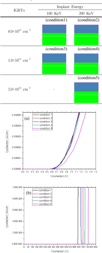
Table 1. Back implant condition result.
IGBTs Implant Energy
180 KeV 200 KeV
8.0×1013 cm-2
(condition1) (condition2)
1.0×1014 cm-2
(condition3) (condition4)
2.0×1014 cm-2 -
(condition5)
(a)
(b)
Fig. 5. Back implant condition simulation (a) on-state voltage drop IcVc graph, (b) breakdown voltage IcVc graph.
(a)
(b)
(c)
Fig. 6. Characteristic of IGBTs (a) break down voltage, (b) on-state voltage drop, (c) threshold voltage.
Table 2. IGBTs of trun-on state voltage drop, breakdown voltage.
IGBTs
Turn-on State Voltage Drop
(V)
Breakdown Voltage
(V)
NPT Planar IGBT 1.45 692
Field Stop Planar
IGBT 1.16 743
3. 결과 및 고찰
그림 5는 N buffer층의 최적 농도를 구하기 위하여 시뮬레이션 한 결과이다. 총 5가지 조건을 시뮬레이션 하였으며, 그 중 가장 최적의 값을 도출 한 결과 값은 1.0×1014 cm-2이다. 그림 6은 앞서 최적 parameter값 을 가지고 설계한 NPT planar IGBT와 field stop planar IGBT의 온 상태 전압강하와 항복 전압을 비 교 분석 하였다. 온 상태 전압강하는 1.45 V, 1.16 V 의 전압 강하를 보이고 있으며 항복전압은 692 V, 743 V를 보여주고 있다.
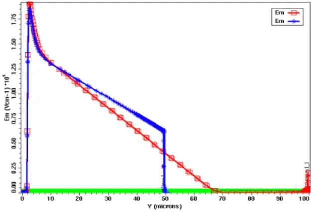
Fig. 7. Planar IGBT VS planar field stop IGBT electric-field graph.
그림 7은 NPT planar IGBT와 field stop IGBT의 전계 분포 그래프이다. NPT IGBT보다 field stop IGBT가 wafer 비저항이 높기 때문에 drift층 영역에 서의 전계 그래프 기울기가 낮은 것을 확인할 수 있 다. 또한 buffer층으로 인하여 전계가 급격히 하락하 는 것을 관찰할 수 있다.
4. 결 론
본 논문은 NPT planar IGBT에 N buffer층을 추가 하는 field stop IGBT를 설계하여 항복전압과 온 상 태 전압강하 특성을 소자 시뮬레이션으로 확인하고 분석하였다. 그 결과 PNT IGBT에 N buffer층을 삽 입한 field stop IGBT의 온 상태 전압강하와 항복전 압이 NPT IGBT보다 미미하지만 향상된 것을 확인 하였다. 또한 N buffer층을 형성시켜 cell depth를
100 u에서 50 um로 줄일 수 있었다. 향후 trench gate를 field stop IGBT에 적용하여 시뮬레이션할 경 우 field stop IGBT의 특성을 더욱 향상시킬 수 있을 것으로 판단된다.
감사의 글
본 논문은 중소기업청 글로벌 강소기업 및 한국연 구재단의 지역혁신 인력 양성사업과 2012년 산학연국 제공동사업으로 수행된 연구결과입니다.
REFERENCES
[1] B. J. Baliga, Power Electronics and Variable Frequency Drives (PWS Publishers, Boston, 1996) [2] E. G. Kang, B. S. Ahn, and T. J, Nam, J. KIEEME,
23, 273 (2010).
[3] J. S. Lee, E. G. Kang, and M. Y, Sung, J.
KEEEME, 19, 912 (2006).
[4] E. G. Kang and M. Y. Sung, J. KIEEME, 13, 371 (2000).
[5] E. G. Kang and M. Y. Sung, J. KIEEME, 15, 758 (2002).