The Software Algorithm Design a Suitable Ultra-Low Power RF System
Jung-won Kim* , Ung-Se Choi * ★
Abstract
The demand of wireless communication is increased rapidly due to the development of wireless communication systems, and many people have the great interest about the ''RF system''. The trend of the RF audio system is to design the system with less power consumption. In this paper, we explain the Software Algorithm Design of RF systems that is suitable for low power consumption.
Keywords: Low power system, RF transceiver, Algorithm
* D ept. of Electr onics En gin eerin g, Korea Polytechnic Graduate School
★
Corresponding author※ Acknowledgment
Manuscript received Feb. 2, 2008 ; published Feb. 27.
2008
I. Introduction
Wireless communications have been evolving very rapidly during past 20 years. At the same time people have increased demands towards them: they want fast, high quality access in every place.
On the other hand demands for services available in wireless networks are same as those for wired ones: everybody wants web browsing, e-mail check, chat but also multimedia services. Multimedia services, which are the topic of this paper, audio streaming have gained much popularity in last years. This has been enabled by the high increase of computing power in home PCs, which allows usage of very efficient audio compression technologies. This paper focuses on testing the possibilities of audio data transfer given by one of the most promising wireless technologies, which is
WPAN(Personal area networks may be wireless with network technologies such as IrDA, Bluetooth, UWB, and ZigBee). WPAN has been designed to replace cable connections between devices like PCs, notebooks, PDAs, phones, headsets, cameras etc.[1,2]
This paper is organised as follows: section 2 describes the principles of the frequency-hopping spread spectrum technology. section 3 describes Software Concept and Design technologies. section 4 contains System Design Progress for Processing a testing environment. This includes The Software Algorithm Design of suitable to ultra-low power RF system. Testbed described in section 4 is used to measure actual RF Current Consumption versus Effective Data Rate and CPU Load versus Effective Data Rate. the last section 5 is ended with summary.
II. Frequency-hopping spread spectrum
Spread spectrum modulation techniques have become more common in recent years. Spread spectrum enables a signal to be transmitted across a frequency band that is much wider than theminimum bandwidth required by the information signal. The transmitter "spreads" the energy, originally concentrated in narrowband, across a number of frequency band channels on a wider electromagnetic spectrum. Benefits include improved privacy, decreased narrowband interference, and increased signal capacity.[3]
In an FH-CDMA system, a transmitter "hops"
between available frequencies according to a specified algorithm, which can be either random or preplanned. The transmitter operates in synchronization with a receiver, which remains tuned to the same center frequency as the transmitter. A short burst of data is transmitted on a narrowband. Then, the transmitter tunes to another frequency and transmits again. The receiver thus is capable of hopping its frequency over a given bandwidth several times a second, transmitting on one frequency for a certain period of time, then hopping to another frequency and transmitting again. Frequency hopping requires a much wider bandwidth than is needed to transmit the same information using only one carrier frequency.[4,5]
The spread spectrum approach that is an alternative to FH-CDMA is direct sequence code division multiple access (DS-CDMA), which chops the data into small pieces and spreads them across the frequency domain. FH-CDMA devices use less power and are generally cheaper, but the performance of DS-CDMA systems is usually better and more reliable. The biggest advantage of frequency hopping lies in the coexistence of several access points in the same area, something not possible with direct sequence.[6,7]
Certain rules govern how frequency-hopping devices are used. In North America, the Industrial, Scientific, and Medial (ISM) waveband is divided into 75 hopping channels, with power transmission not to exceed 1 watt on each channel. These restrictions ensure that a single device does not consume too much bandwidth or linger too long on a single frequency.[8,9]
III. Software Concept and Design
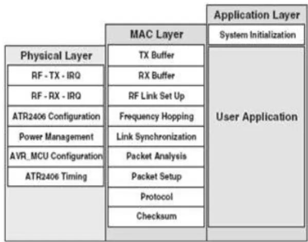
The RF firmware implements three main layers to set up the RF link and to exchange data via RF T h e l o w e s t l a y e r ( t h e p h y s i c a l l a y e r ) i s responsible for the exchange of the RF data and the configuration of the transceiver. The second layer (the MAC layer) handles the transmit and receive buffers, holding the RF data. The MAC l a yer a l so gen er a tes the tim in g n eeded to control the RF chip, and analyzes the received packet and the setup of a response packet.
Fig. 3-1. Software Concept
T h e t o p la y er o f t h e R F f i r m wa r e ( t h e application layer) serves the special needs of the application and is completely independent of all the RF-related tasks. This independence makes it easy to implement the application layer, as the user does not need to worry about anything related to the RF task, unless the application uses other interrupt sources. To realize the RF specific tasks, some hardware resources of the microcontroller are needed. These resources include two peripherals, the USART interface and one timer, as well as Flash and RAM. About 1000 instruction words of Flash are necessary, and 140 bytes of RAM, which
is due mostly to the RX and TX buffers for the RF data. The rest of the MCU peripherals and memories can be freely used by the application-specific tasks.
The chosen software concept is shown in Figure 3-2. The boxes include all the necessary function blocks needed to implement a simple point-to-point RF link. The software is kept flexible for chosen net topology. The software serves not only for point-to-point connections, but it is also easily adaptable for multiple point-to-point RF links. To exchange packets via the RF link the user has only to work with the RX/TX buffers. To transmit data, the data needs to be written into the TX buffer. All the rest is done automatically by the RF firmware. If the data has been written into the TX buffer, the Microprocessor can calculate a CRC-16 checksum for the data to be transmitted.
The transmission of the whole data is interrupt driven.
Because of the high data rate this interrupt handler has to be very fast. Therefore it is written in assembler. While transmitting a packet the system performance is lowered to 60%. This value seems to be low, but in a typical RF link the transceiver transmits only every few milliseconds. Another point is that because of the high data rate, the transmission time is very short.
Fig. 3-2. RF Firmware Concept
The reception of data is also completely controlled through the RF firmware. The user can poll a flag
to see if new data was received. The data is stored in the RX buffer. To check if the packet is okay it is also possible to calculate a CRC-16 check for the received data. While receiving, the CPU performance is lowered to 55%.
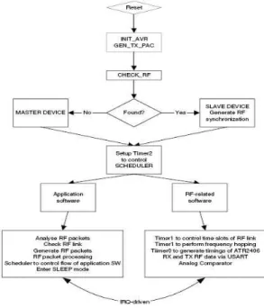
III-I. RF Software Flow
For ease of comprehension Figure 3-3 shows a typical software flow for the reception of RF data and the reception of a packet is explained. Reception is started automatically through Timer1 with the execution of “pwr_up_rf(RXEN)”. This timer is used to keep the whole system synchronized in time and on the same channel (Frequency hopping system).
Fig. 3-3 Software Flow
First Timer0 is enabled to generate, like in transmit mode, the needed timings for the configuration of the transceiver , the settling time of the loop filter and the power up sequence of the ISM transceiver.
In the next step the USART is enabled to receive the RF data. When a valid address is received
RF Task Application Task 16 bit Timer Two 8 bit Timer
No EEPROM Complete EEPROM
2KByte Flash 2KB/6KB/14KB of
Flash 154 Byte of SRAM (depends
mainly on RF buffer length) 454 Bytes/ 970 Bytes of SRAM
USART interface SPI Binterface, all ADC
8 GPIOs 13 GPIOs
TWI interface,all PWM watchdog timer during the opened receive window the receive interrupt is enabled. This interrupt stores the received bytes in the RX buffer until an end of packet qualifier is received. At the end the whole receive machine is disabled and a flag tells the application software that new data has been received. Another important step, done while receiving the packet, is the generation of a timestamp. This timestamp is taken after each reception of a valid address and becomes valid if the received packet is thought to be correct. Now this timestamp is used to keep the slave system synchronized to the master device. Only slave devices have to resynchronize to the master clock.
To detect errors in the RF link as early as possible, the most common easily recognizable errors are detected in the receive interrupt handler, such as a buffer overrun or a timeout of the receive window.
The RF firmware requires some RAM and Flash memory, as well as some peripheral support.
Table 3-1 Microprocessor Resources
The necessary Flash space for a minimal implementation of the RF firmware is about 1120 words (2240 Bytes), about 55% of the Flash size of an micorprocessor, the smallest available microprocessor. This Flash space includes the required “C Start up”, without which the size of the code is reduced to only 1000 words (2000 Bytes),
meaning that the RF firmware itself is only about 49% of the space available in an micorprocessor. To achieve high system performance the RF task is supported by two peripherals, the USART and Timer1. Timer1 is used to generate all the needed RF timings and the USART is used to exchange RF data between the micorprocessor and the Transceiver.
There are eight I/O lines needed to control the Transceiver. To achieve this low I/O usage some of the signals have to be connected together, or eleven I/O lines would be needed.
IV. System Design Progress Process
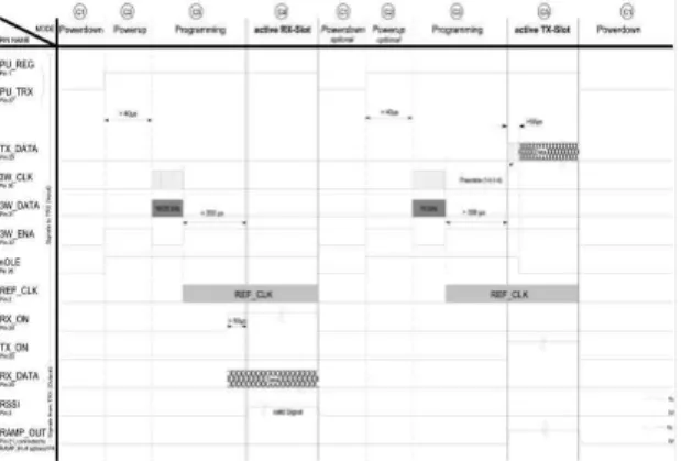
The organization of the RF time slots is shown in Figure 4-1. The figure is based on an example that uses a slot time of 10 ms, that means the device transmits every 20 ms a packet and also each 20 ms a packet will be received. The slot time is the time difference between transmitting and receiving a packet via RF. Regarding Figure 4-1, there are five different periods of time. The time from power down untill ready to transmit data is the complete time needed to power up and configure the transceiver including the period of time needed by the loop filter to settle. The same applies for the transceiver used in receive mode. Both tasks need the same amount of time, 395 μs.
Fig. 4-1. RF Slot Timing
This will result in a faster settling time of the filter, but the time used to exchange data via RF will also be lowered. The active data slot to transmit data depends on the length of the transmitted packet. A very important point is the receive data slot pre-setting. This period of time is needed to keep the system in synchronization, even if several packets are lost (synchronization is only started after the reception of a correct packet).
Fig. 4-2. RX & TX Timing Diagram
Starting from power down mode, U_REG & PUTRX are toggled to high about 40us in advance to 3-wire programming. After performing the 3-wire programming the loop needs to settle frequency.
TX_ON is toggled to high about >200us after the PLL-programming. After performing the 3-wire programming, the loop needs to settle frequency.
RX_ON is toggled to high about 150μs after PLL-programming.
A very important item concerning wireless systems is the current consumption. A main factor influencing the current consumption is the effective data rate that has to be transmitted via RF.
Another factor influencing the current consumption is how many bursts per second are used to exchange the data. Figure 4-3. shows a diagram displaying the relationship between consumed current, effective data rate and the number of burst per second.
Fig. 4-3. RF Current Consumption versus Effective Data Rate
The CPU load caused by the transmission and reception of data v RF depends on how many bits per second are exchangiaed and how many bursts are used to do this. Figure 4-4 illustrates this by showing two possible operating modes. A mode, in this case, means how many bursts per second are exchanged.
Fig. 4-4. CPU Load versus Effective Data Rate
The default RF data rate of the RF firmware is 1.152 Mbps. But it is also possible to lower the RF data rate (576 kbps, 288 kbps, 144 kbps). If such
Parameter after before CPU power needed for
RX 33% 52%
CPU power needed for
TX 30% 50%
RF slot time 2000μs 4200μs
TX @100kbit/s, typ. 6mA 9mA
Stand-by 0.9μA 1.3uA
lower data rates are needed. An important fact regarding the USART and the required RF data rate is that the USART has to be configured in synchronous mode when using the 1.152 Mbps. All the other possible data rates do not work with the synchronous USART. In these cases the USART has to be used in asynchronous mode. The reason for this is that the clock recovery feature can only be used at the highest data rate. In all other cases (lower data rates) this feature cannot be used. To configure the USART in asynchronous mode, the user has only to change the register settings of the USART to the desired behavior. The usage of the asynchronous USART also needs another change to the RF firmware. The configuration of the ISM transceiver chip has to be changed. When in default the chip is configured to generate the recovered clock while receiving data via RF. Therefore, the configuration word to put the transceiver into receive mode has to be changed to 16 bits as in the case of transmit. Lowering the RF data rate has some disadvantages, for example, the higher power consumption of the system as the exchange of data needs more time and therefore the transceiver has to be powered up for a longer period of time.
Depending on the packet length the receive window length should also be adjusted.
RF firmware is system performance, to give the application as much of the CPU power as possible to deal with the application specific tasks. For a better understanding of the numbers given in the features list of the RF firmware, see this result.
Table 4-1 RF firmware performance
So, 360 μs are needed to deal with the RF-related
tasks in a complete time of 4000 μs. Therefore, the average necessary CPU power to achieve an effective average data rate of 192 Kbps is 360 μ s/4000 μs = 9.0%.
V. Conclusion
In this paper we designed a Software Algorithm a suitable ultra-low power RF system. to give the application as much of the CPU power as possible to deal with the application specific tasks. the average necessary CPU power to average 9.0%.
Now, it is also necessary to include the CPU power needed to handle the Timer1 interrupt. Roughly, for the whole RF task, 10% of CPU power is needed.
That means the application software has up to 90%
of CPU power to serve its special needs.
2.4-GHz Smart RF transceiver and the microcontroller. The proprietary Smart RF firmware implements an adaptive frequency-hopping protocol, enabling robust and reliable data transmission even in a noisy RF environment with interfering signals from WLAN, Bluetooth, Zigbee. The Firmware design is especially designed to meet the performance and cost requirements of wireless game controllers, but also addresses other wire-replacement applications in the consumer area, such as wireless audio links, interactive intelligent toys and remote controls.
References
[1] IEEE Std. 802.15.1, “Wireless Medium Access Control(MAC) and Physical Layer(PHY) Specifications for Wireless Personal Area Networks(WPANs),” 2002.
[2] Mobile Networking LAB. POSTECH http://anmc.postech.ac.kr/research.html#wpan
[3] ISSCE-Circuits Systems, “Principles of SpreadSpectrum Communication"
target="new">http://olt.tudelf.nl/~glas/ssc/techn/t
echniques.html
[4] Internet Magazine. "Spread Spectrum Scene"
ABC's of Spread Spectrum",
http://sss-mag.com/ss.html
[5] frequency-hopping spread spectrum Web site http://blog.naver.com/chroma14/90017782583 [6] Hoe-sam Jeong, The transceiver structure of
Bluetooth suitable to ultra-low power home network system, Telecommunications Review·
Vol.14 No.2,·Apr.2004.
[7] Jeyhan Karaoux, “High-Rate Wireless Personal Area Networks,” IEEE Communications Magazine,” Vol.39 No.12, Dec. 2001.
[8] Theodore B. Zahariadis, et al., “Global Roaming in Next-Generation Networks,” IEEE
Communications Magazine, Feb. 2002.
[9] Robert Berezdivin, Robert Breinig, and Randy Topp, Raytheon, “Next-Generation Wireless Communications Concepts and Technologies,”
IEEE Communications Magazine, Mar. 2002.
BIOGRAPHY
Jung-won Kim (Number)2002 : BS degree in Electrical Engineering, Korea Polytechnic University.
2004 : MS degree in Electrical Engineering, Korea Polytechnic University.
2008 : PhD courses at Electrical Engineering, Korea Polytechnic University.
2001~2004 : Research Engineer, Namsong Ind.
2004~ : Research Engineer, Changnam I.N.T
Ung-se Choi (Nember)
1981 : BS degree in Electronics Engineering, Myong-Ji University.
1983 : MS degree in Electronics Engineering, Myong-Ji University.
1995 : PhD degree in Electronics Engineering, Myong-Ji University.
1981~1997 : Advanced Research Engineer, KITECH.
1997~ : Professor, Department of Electronics Enginnering, Korea Polytechnic University