1
UV/O 3 조사 시간에 따른 Sol-gel 공정 기반 CuO 박막 트랜지스터의 전기적 특성 변화
UV/O 3 Process Time Effect on Electrical
Characteristics of Sol-gel Processed CuO Thin Film Transistor
이 소 정 * , 장 봉 호 * , 김 태 균 * , 이 원 용 * , 장 재 원 * ★ Sojeong Lee * , Bongho Jang * , Taegyun Kim * , Won-Yong Lee * , Jaewon Jang * ★
Abstract
In this research, sol-gel processed CuO p-type thin film transistors were fabricated with copper (II) acetate monohydrate precursors. After 500 ℃annealing process, the deposited thin films were fully converted into CuO.
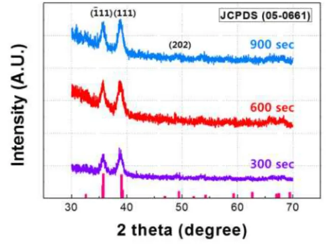
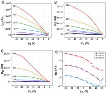
We investigated UV/O 3 process time effect on electrical characteristics of sol-gel processed CuO thin film transistors. After 600 sec UV/O 3 process, the fabricated CuO thin film transistor delivered field effect mobility in saturation regime of 5 × 10 -3 cm 2 /V·s and on/off current ratio of ~10 2 .
요 약
Sol-gel 공법을 이용하여, p-형 CuO 박막 트랜지스터를 제작하였다. 제작된 CuO 박막 트랜지스터는 copper (II) acetate
monohydrate 를 전구체로 사용하였다. 500
℃열처리 후에 형성된 전구체는 p-형 CuO 박막이 됨을 확인하였다. 또한 전
구체를 형성하기 전 기판표면의 UV/O 3 조사량에 따른 CuO 박막 트랜지스터의 전기적 특성변화에 대하여 연구하였
으며, 600 초동안 UV/O 3 를 조사한 경우 제작된 CuO 박막 트랜지스터는 5 × 10 -3 cm 2 /V·s 의 이동도와 약 10 2 의 온/오프 전류비를 보여주었다.
Key words : Sol-gel, CuO, UV/O 3 , p-type semiconductor, Thin film transistor
* School of Electronics Engineering, Kyungpook National University,
★ Corresponding author
※ Acknowledgment
This research was supported by Basic Science Research Program through the National Research Foundation of Korea (NRF) funded by the Ministry of Education
(NRF-2016R1D1A3B03930896)
Manuscript received Feb. 26, 2018; revised Mar. 18, 2018 ; accepted Mar. 20, 2018
This is an Open-Access article distributed under the terms of the Creative Commons Attribution Non-Commercial License (http://creativecommons.org/licenses/by-nc/3.0) which permits unrestricted non-commercial use, distribution, and reproduction in any medium, provided the original work is properly cited.
Ⅰ. 서론
최근 용액 공정 기반의 산화물 반도체에 대한
연구가 많은 관심을 받고 있다 [1]. 상대적으로 큰
밴드갭을 가지며, 우수한 전기적 특성을 보여주는
동시에 기존의 진공 증착 방법이 아닌 용액 공정
을 통하여 저비용으로 대면적 소자를 제작하는데
적합한 물질로 주목을 받고 있다 [2],[3]. 특히
ZnO, In 2 O 3 , 및 SnO 2 은 대표적인 n-형 반도체
물질로, 이를 이용한 다양한 방법의 고성능 투명
트랜지스터가 제작되기도 하였다. 일반적으로
n-type 산화물 반도체 기반의 트랜지스터의 경우
고전류, 고이동도, 및 높은 온/오프 전류비 등으로
인하여 차세대 투명 소자의 핵심 단위 소자로