- 122 -
Fabrication of Magnesium Diboride Thin Films by Aerosol Deposition
B. B. Sinhaa, K. C. Chung*,a, S. H. Janga, B. D. Hahna, D. S. Parka, X. L. Wangb, S. X. Doub
a Korea Institute of Materials Science, 797 Changwondaero, Changwon, 642-831, Korea
b Institute for Superconducting and Electronic Materials, Univ. of Wollongong, NSW2500, Australia (Received 31 October 2011 revised 20 December 2011 accepted 23 December 2011)
에어로졸 증착법에 의한 MgB
2박막 제조
B. B. Sinhaa, 정국채*,a, 장세훈a, 한병동a, 박동수a, X. L. Wangb, S. X. Doub
Abstract
Superconducting MgB2 thin films were fabricated by using a novel aerosol deposition technique wherein the pre-reacted powder is directly transformed into respective thin film. The formed thin films were characterized by X-ray diffraction technique and FE-SEM to understand its structure and morphology and the superconducting behavior has been characterized with the four probe resistivity measurement. The as-deposited thin films were formed into the frustrated amorphous structure, which were relaxed on the further heat treatment at 900 °C for 3 hrs. The relaxed amorphous MgB2 thin films showed a comparatively high superconducting onset at about 38 K.
Keywords : MgB2, aerosol deposition, superconductor
I. Introduction
Magnesium diboride is a binary intermetallic superconductor which catches the interest among the modern day technologies for the fabrication of superconducting tapes and wires. Having the highest transition temperature of 39 K amongst the simple binary intermetallic superconductors, it is considered as a low cost substitute of the currently used Nb based superconductors. Since the discovery of
superconductivity of MgB2 in 2001 [1], various methods were employed for the synthesis in different forms [2-6]. MgB2 has many synthesis related problems such as difference in melting point of Mg and B, high vapor pressure of Mg, formation of MgO etc. Hence synthesis of MgB2 requires inert atmosphere to prevent oxidation along with high Mg pressure to compensate for the possible loss of Mg.
Further thin film synthesis by physical vapor deposition requires good vacuum but at the same time high vacuum reduces the decomposition temperature drastically [7-8]. Thus the cost effective and easy fabrication of MgB2 thin films has been
*Corresponding author. Fax : +82 55 280 3392 e-mail : [email protected]
thought as difficult [9]. Although thin film synthesis of MgB2 is difficult, various applications such as tunneling devices demands the fabrication of good quality superconducting films, that may replace the low transition temperature superconducting materials like Nb3Sn and NbTi.
There are various techniques for the synthesis of MgB2 thin films out of which the best method to fabricate good quality thin films is the Mg diffusion method [10]. This technique requires maintaining stringent conditions such as proper Mg vapor pressure, annealing in a vacuum sealed tube, optimized annealing temperature under proper pressure to prevent the decomposition of the synthesized films etc. This approach of thin film synthesis is a kind of bottom up approach in which the films are formed from different precursors of Mg and B which can react under carefully maintained conditions. These methods are excellent in terms of formations of MgB2 thin films but are somewhat unrealistic in terms of mass production.
In this paper we discuss a kind of top to bottom approach in which the MgB2 thin films are deposited directly using a pre-reacted MgB2 powder. This is achieved by a novel technique called Aerosol Deposition (AD) technique wherein the precursor powder particles are smashed on to the substrate in such a way that the force of impact on the substrate results into consolidated thin film. This technique was developed for the room temperature deposition of dense ceramic films [11]. AD has been successfully used to deposit ceramic powders such as Al2O3 [12], Y2O3, TiO2, PZT [13] etc. targeting the applications like micro-actuators [14], high frequency devices [15], high speed optical modulators [16], solid oxide fuel cells [17], and conductometric bulk sensors [18]. So far to our knowledge AD was hardly used for the fabrication of the superconducting films. We are for the first time reporting the fabrication of amorphous MgB2
superconducting thin films.
II. Experimental
Superconducting magnesium diboride thin films were successfully fabricated by a novel aerosol deposition (AD) technique by using indigenously built AD setup. The deposition was carried out on single side polished (0001) Al2O3 substrate using pre-reacted high purity MgB2 powder from Alpha Aesar. The aerosol deposition was carried out by using a nozzle of dimension 3.5 mm x 0.5 mm. The MgB2 powder was accelerated by the carrier gas flow of 30 liters per minute as controlled by the mass flow controller. The substrate to nozzle distance was maintained at 5mm to obtain the optimum deposition.
The mixed gas of Ar + 4 % H2 was used as a carrier with a view of creating reducing environment for the prevention of possible oxidation of MgB2 powder during the deposition process. The whole deposition chamber was continuously evacuated by a combination of booster and rotary pump in order to maintain the pressure difference between the deposition chamber and the powder container.
The highly adherent as-deposited films were heat treated at 900 oC for 3 hrs under Ar + 4 % H2
environment in the presence of magnesium. The as-deposited as well as the heat treated films were characterized by X-ray diffraction for its structural determination. The quality of the films in terms of its surface morphology was understood by FE-SEM studies. These films were then subjected to resistivity measurements in order to study its superconducting behavior in terms of transition temperature using Quantum Design PPMS model 6000.
III. Results and Discussion
Fig. 1(a) shows the X-ray diffraction patterns for the MgB2 thin films deposited on alumina single crystal substrates where the intensity is plotted in log scale. Here the as-purchased MgB2 powder was subjected to the aerosol deposition with the carrier gas flow rate of 30 L/min and substrate to nozzle distance was maintained at 5 mm. The XRD analysis
of the as-deposited thin films showed the very high intense peak for alumina substrate. It is interesting to observe hardly any peaks for the MgB2 phase except for (001) and (002) peaks. This suggests that the formed MgB2 thin film is more or less amorphous in nature. The c-axis oriented peaks for MgB2 are not as intense to be considered as the preferred orientation.
Fig. 1. XRD patterns of (a) as-deposited MgB2 thin films and (b) MgB2 powder from the aerosol deposition chamber.
In this case the substrate was maintained at room temperature under high carrier gas (with MgB2
precursor powder) flow atmosphere and a small impact distance. Under this condition, the powder particles would have undergone an impact on substrate with a high kinetic energy enough to get fractured and loose its structure. Further, there is very less time and insufficient energy for recovery and
re-crystallization before the next powder particles’
impact, resulting in a very small amount of c-axis orientation taken from the substrate. This leads to the formation of a frustrated amorphous structure without sufficient relaxation for proper lattice formation. Although the deposited thin film seems to be amorphous, it is interesting to know that the scattered powder in the chamber showed the perfect crystal structure for MgB2 as seen from Fig. 1(b).
This may prove that only the powder particles having sufficient impact energy on the substrate gets fractured into smaller particles and adhered to substrate while the rest gets rejected.
Fig. 2. Field emission gun scanning electron microscope images of aerosol deposited thin films at (a) 1X, (c) 10X and (d) 60X magnification. (b) FE-SEM images of precursor MgB2 powder used for AD.
It is well supported from the FE-SEM images for the films and the precursor powder as shown in Fig. 2 (a) and (b). Fig. 2(a) shows the image for the as-deposited MgB2 thin films while the image for the precursor powder is as shown in Fig. 2(b). It can be clearly seen that the precursor powder has the particles with the size of around 50 μm while the films appears to be quite continuous without any signature of discrete nature of particles. This supports our argument that the impact occurred in the AD process fractures the powder particles resulting into compact solidification on the surface of the substrate.
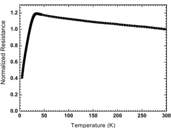
Fig. 3. Resistivity behavior of the as-deposited MgB2 thin films in terms of normalized resistance with respect to temperature.
Fig. 4. X-ray diffraction pattern of the MgB2 thin films annealed at 900 °C for 3 hrs.
This is in line with the XRD measurements where no major peaks for the MgB2 phase are observed, depicting more or less amorphous nature of the film.
The more magnified images of thin film are shown in Fig. 2(c) & (d). From these images it can be understood that the surface appears to be discrete with a bit poor connectivity amongst the grains. This was reflected in the transport studies performed on the as-synthesized MgB2 thin films.
Fig. 3 shows the behavior of normalized resistance as a function of temperature. It can be seen that the resistance goes on increasing with the decrease in the temperature thus following a semiconducting nature.
This is due to the poor continuity amongst the frustrated network of grains. The increase in resistance was observed up to 32 K beyond which there was a sharp decrease up to 5 K. This decrease in the resistance was observed as magnesium diboride went into a superconducting state. This incomplete transition observed is in agreement with the fact that there is poor grain connectivity in the as-deposited MgB2 film as shown in Fig. 2(d).
To further enhance the intergrain connectivity, the as-deposited MgB2 films were annealed in Mg environment at 900 °C for 3 hrs. Although there was barely any change in the amorphous nature of the films, it showed some sign of recovery and rearrangement in the MgB2 lattice as evident from the appearance of low intensity (101) peak in Fig. 4.
Fig. 5. Resistivity behavior of the annealed MgB2 thin films in terms of normalized resistance with respect to temperature.
A remarkable improvement in the intergrain connectivity was observed in the MgB2 film after heat treatment. It reflected in the resistivity behavior of the film as may be seen from Fig. 5. In comparison, the heat treated MgB2 film showed a metallic behavior as against the semiconducting nature for the as-deposited MgB2 film. The resistance decreased with the decrease in temperature up to 37.8 K where it showed onset of superconducting transition. The complete transition was observed only at 28 K with a broad transition. Such a broad transition observed is
0 50 100 150 200 250 300
0.0 0.2 0.4 0.6 0.8 1.0 1.2
Normalized Resistance
Temperature (K)
20 30 40 50 60 70 80
10 100 1000
10000 A D 305H
* Al2O3 * Al2O3
MgO
Mg
2θ (deg)
Log of Intensity (A.U.) * Al2O3 (002) MgB2 * Al2O3
(101) MgB2
0 50 100 150 200 250 300
0.0 0.2 0.4 0.6 0.8 1.0
20 30 40
0.0 0.2 0.4 0.6 0.8 1.0
Normalized resistance
Tem perature (K)
Normalized Resistance
Tem perature (K) TOnsetc = 37.8K
TOffsetc = 28K
in agreement to the XRD measurements, which showed the amorphous structure of the MgB2 film that result into increased carrier scattering.
IV. Summary
Aerosol deposition was successfully used to synthesize superconducting MgB2 thin films. The deposition was carried out by using pre-reacted MgB2 powder which eliminates the requirement of the complex and stringent heat treatment conditions for the formation of the MgB2 phase. High impact of the powder particles on the substrate during the deposition resulted in to fracture of the particles giving rise to the frustrated amorphous thin films.
Heat treatment is required to relax the frustrated structure which resulted into good grain connectivity and ultimately complete superconductivity in the MgB2 films at about 28 K. The broad transition from 38 K to 28 K was observed due to the disordered nature films which can be improved by proper annealing of the film.
Acknowledgments
This work was supported by the Global Research Laboratory program (M60602000012) from the National Research Foundation of Korea through a grant provided by the Korean Ministry of Education, Science & Technology (MEST).
References
[1] J. Nagamatsu, N. Nakagawa, T. Muranaka, Y.
Zenitani and J. Akimitsu, Nature 410 (2001) 63.
[2] K.H.P. Kim, J.H. Choi, C.U. Jung, P. Chowdhury, H.S. Lee, M.S. Park, H.J. Kim, J.Y. Kim, Z. Du, E.M.
Choi, M.S. Kim, W.N. Kang, S.I. Lee, G.Y. Sung, J.Y.
Lee, Phys. Rev. B, 65 100510 (2002).
[3] Y. Takano et al., unpublished; A.K. Pradhan, Z.X. Shi, M. Tokunaga, T. Tamegai, Y. Takano, K. Togano, H.
Kito, H. Ihara, Phys. Rev. B 64 212509 (2001).
[4] Y. Takano et al., unpublished; A.K. Pradhan, Z.X. Shi, M. Tokunaga, T. Tamegai, Y. Takano, K. Togano, H.
Kito, H. Ihara, Phys. Rev. B 65 144513 (2002).
[5] S. Okuma S. Togo and K. Amemori, Phy. Rev. B 67 172508 (2003).
[6] B A Glowacki, M Majoros, M Vickers, J E Evetts, Y Shi and I McDougall, Supercond. Sci. Technol. 14 193 (2001).
[7] A. Handstein, D. Hinz, G. Fuchs, K.H. Muller, K.
Nenkov, O. Gutfleisch, V.N. Narozhnyi, and L.
Schultz, J. Alloys Compd. 329 285 (2001).
[8] Z.K. Liu and D.G. Schlom, Appl. Phys. Lett. 78(23) 3678 (2001).
[9] C. Buzea and T. Yamashita, Supercond. Sci. Technol.
14 R115 (2001).
[10] Z.K. Liu, D.G. Schlom, Q. Li and X.X. Xi, Appl.
Phys. Sett. 78, 3678 (2001).
[11] J. Akedo, M. Lebedev, Jpn. J. Appl. Phys. 38 5379 (1999).
[12] S.M. Nam, N. Mori, H. Kakemoto, S. Wada, J. Akedo and T. Tsurumi Jpn. J. Appl. Phys., 43, 5414 (2004).
[13] N. Asai, R. Matsuda, M. Watanabe, H. Takayama, S.Yamada, A. Mase, M. Shikida, K. Sato, M.
Lebedev and J. Akedo, Proc. Of IEEE MicroElectro Mechanical Systems, pp. 247-50.
[14] J. Akedo and M. Lebedev, Appl. Phys. Let. 77-11, 1710 (2000).
[15] Y. Imanaka, M. Takenouchia and J. Akedo J. Cryst.
Growth 275, 1313 (2005).
[16] J. Akedo, M. Lebedev, H.Sato, and J. Park, Jpn. J.
Appl. Phys. 44 7072 (2005).
[17] J. Choi, J. Lee, D. Park, B. Hahn, W. Yoon, H. Lin, J.
Am. Ceram. Soc. 90 1926 (2007).
[18] K. Sahner, M. Kaspar and R. Moos, Sens. Actuators B. Chem. 139 394 (2009).