New Physics: Sae Mulli,
Vol. 69, No. 5, May 2019, pp. 458∼461 http://dx.doi.org/10.3938/NPSM.69.458
Electron-Beam-Assisted Low-Temperature Crystallization of CuInSe
2Maeng Jun Kim
Korea Multi-purpose Accelerator Complex, Korea Atomic Energy Research Institute, Kyungju 38180, Korea
Sung Youp Lee · Hyeong Rag Lee · Sang Ho Sohn
∗Department of Physics, Kyungpook National University, Daegu 41566, Korea (Received 11 December 2018 : revised 22 February 2019 : accepted 11 March 2019)
The effects of electron-beam (E-beam) irradiation on the formation of CuInSe2 (CIS) thin films were investigated through a structural characterization of amorphous CIS (a-CIS) thin-films co- evaporated onto glass substrates. A-CIS thin-films were either heat-treated or subjected to E-beam irradiation. With the E-beam treatment, the crystallization temperature significantly decreased.
This is probably due to the catalytic effect of the electrons reducing the activation energy and promoting the nucleation and growth of crystallite grains. The results imply that crystallization can be promoted by using an electron-mediated catalytic effect. The findings in this study open the way for low-temperature crystallization of CIS thin films.
PACS numbers: 61.05.-a, 64.60.-i
Keywords: CIS, Crystallization, E-beam, Solar cell
I. INTRODUCTION
In recent years, the use of CuInSe2(CIS) thin films (as the absorption layer) in solar cells has attracted much at- tention due to its wide band gap [1–3], high absorption coefficient, broad spectrum absorption, and high ther- mal stability [4]. Owing to its larger grain sizes, crystal- lized CIS is superior to as-deposited films from aspects of electronic and material properties, but the crystallization of CIS films usually requires a heat treatment of up to 500°C. However, such high temperatures are not suitable for fabrication of CIS films on polymer foils (that have low melting points) and therefore, an alternative route is required. Recently, in a polymer foil based solar cell fabricated by a low-temperature process, the efficiency of 20.4 % was reported [5]. Although low temperature processing techniques continue to be developed, they are currently confined to thermal annealing methods. As a promising low temperature alternative to this, the metal- induced crystallization of a-Si to poly-Si is introduced
∗E-mail: [email protected]
[6]. Other methods available to reduce the crystalliza- tion temperature of CIS are still in need. In this study, we investigated electron-beam (E-beam) assisted crys- tallization of CIS thin films at low temperatures with a focus on the structural and morphological properties of thin films. The results are compared to those obtained in conventional thermal annealed specimens.
II. EXPERIMENTAL SETUP
Five a-CIS films were grown on Corning 7059 glass using a co-evaporation system operated under ultrahigh vacuum changing from 10−8 to 10−7 Torr according to the source flux and substrate temperatures. The Cu, In, and Se sources were granular with purity of 99.999% and the amorphous CIS (a-CIS) films had an atomic compo- sition ratio of [Se]:[Cu]:[In] = 2.2:1:1 to within an error of 0.1%, as measured by inductively coupled plasma-atomic emission spectroscopy (ICP-AES). The overall thickness of the five films was fixed at 1 µm.
This is an Open Access article distributed under the terms of the Creative Commons Attribution Non-Commercial License (http://creativecommons.org/licenses/by-nc/3.0) which permits unrestricted non-commercial use, distribution, and reproduction in any medium, provided the original work is properly cited.
Electron-Beam-Assisted Low-Temperature Crystallization of CuInSe2 – Maeng Jun Kim· Sung Youp Lee 459
High Temperature X-Ray Diffraction (HT-XRD) was performed with a diffractometer comprised of a PANalyt- ical Pro-MPD θ/θ goniometer, a chamber furnace (An- ton Paar HTK 16) and a PIXcel linear position-sensitive detector (LPSD). The 2θ range was 10-70°. Each of the prepared films was mounted on a Pt strip heater with carbon paint to provide an improved thermal contact.
The temperature of the heating area was regulated with a PID controller and measured by an S-type thermocou- ple welded to the bottom of the heater. Steps -ramp an- nealing were performed in order to investigate the phase evolution of the samples. XRD measurements were per- formed over the temperature ranges of 25–550°C by a step-ramp annealing with increment of 20°C and heat- ing rate of 30°C/min in a flowing He atmosphere [7].
The phase transition was studied by monitoring the evo- lution of characteristic peaks in the XRD patterns of the step-ramp annealed samples. In addition, morphologi- cal studies were performed with scanning electron mi- croscopy (SEM).
The a-CIS films were also subjected to E-beam irra- diation. The E-beam equipments including the power supply used for E-beam irradiation is commercially avail- able from BOC Coating Technology. Sample is put on alumina crucible. In order to prevent local heating and damage on specimens, raster scanning system is used via 1 Hz. Treatment time is about 5 minute. A nominal op- eration power condition is 7 kV, 0.5 A. We could not measure exact spot size and density distribution. But with eye observation, it reaches about 1∼3 mm diame- ter.
To employ the E-beam method for the low tempera- ture preparation of crystallized CIS (c-CIS) thin films, it is important to monitor the temperatures that the speci- men is exposed to the electron bombardment. Therefore, we exposed commercially available temperature indicat- ing strips to the E-beam under the same experimental conditions as specimens were prepared. The surface tem- perature generated by the E-beam was found to range from 166°C to 171°C. Further confirmation of the tem- perature was done by depositing the a-CIS films on PET film substrates. The PET film substrates with a melting point of 230°C were subjected to irradiation of E-beam under the same conditions as those used to prepare the specimen with glass substrates. After E-beam treatment,
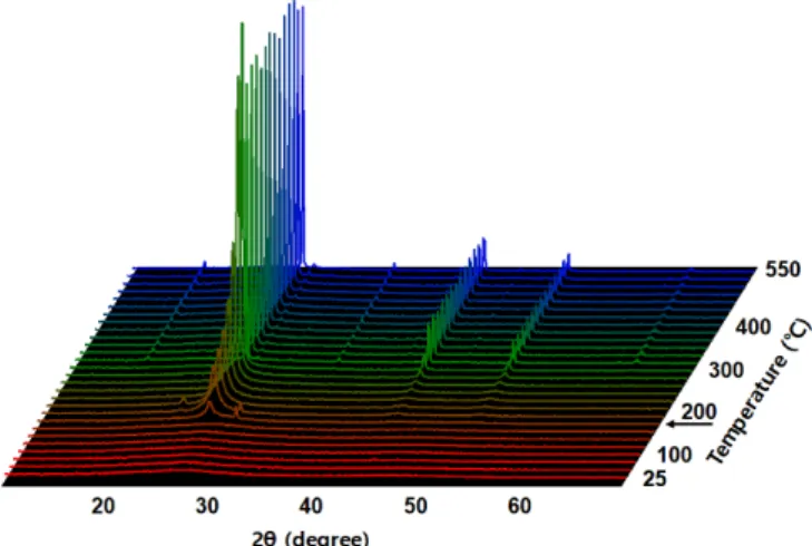
Fig. 1. (Color online) In situ HT-XRD patterns of the a-CIS films during the step-ramp annealing process.
crystallization still proceeded without melting of PET as confirmed with SEM. This fact corroborates that the temperatures during the E-beam treatment never exceed 230°C.
III. RESULTS AND DISCUSSION
Fig. 1 shows the XRD patterns of the a-CIS films.
Step-ramp annealing caused an a-CIS to polycrystalline CIS (poly-CIS) phase. It is confirmed that a dramatic CIS crystallization including the transitional phase of In2Se3 and Cu2Se at 28.3° and 23.1°, respectively oc- curs. This suggests that the main crystallization process is driven by the Cu2Se + In2Se3CuInSe2reaction mecha- nism. The XRD data observed at 160°C (indicated by an arrow in Fig. 1) exhibit the formation of a poly-CIS phase (rather than being fully crystallized) accompanied by a nucleation process. At around 400°C, the film is fully crystallized, showing no additional decrease in the full width at half maximum (FWHM) and saturation of the integrated area of the Gaussian fits to the main peaks.
Figure 2 shows cross-sectional SEM images of: (a) the as-deposited a-CIS films, (b) after a complete ramp an- nealing to 550°C and (c) an E-beam treated film. As can be seen in Fig. 2(a), the morphology of the a-CIS film does not indicate crystallization. Contrary to this, the E-beam treated specimen evidently shows fully crystal- lized film structures and large grains of the order of the film thickness. Any differences in morphologies of the
460 New Physics: Sae Mulli, Vol. 69, No. 5, May 2019
Fig. 2. Cross-sectional SEM images of (a) as-deposited a-CIS films, (b) CIS films after a complete step-ramp annealing process to 550°C, and (c) the E-beam treated CIS films.
E-beam enhanced and conventionally heat-treated spec- imens (Figs. 2(b) & (c)) are difficult to distinguish.
The structural characterization of samples by XRD is shown in Fig. 3. Contrary to the a-CIS films showing only one broad peak, the E-beam treated films illustrated sharp peaks originated from the tetragonal CIS phases, which are similar to those seen in the ramp-annealed specimen at 550°C as shown in Fig. 3(b). The strongest XRD peak was observed at 2θ = 26.6°, which is associ-
Fig. 3. (Color online) XRD patterns for (a) the as- deposited a-CIS films and E-beam treated specimen, and (b) the step-ramp annealed films to 160°C and 550°C.
ated with the tetragonal (112) plane. The peaks at 2θ = 44.1° and 44.2° are associated with the tetragonal (204) and (220) planes, respectively while the peaks at 2θ = 52.2° and 52.3° are associated with the tetragonal (116) and (312) planes, respectively. The degree of crystal- lization detected by the XRD measurements is in agree- ment with the SEM images seen in Fig. 2. XRD pattern obtained from the samples suffering from the step-ramp process to 160°C is also shown in Fig. 3(b). This temper- ature (160°C) was chosen because, as described above, it is close to the actual temperature reached during E- beam bombardment. In this case, the absence of the characteristic satellite peaks indicates that even though the thermal energy available at 160°C might initiate the crystallization process of the a-CIS film, it does not com- plete it.
Electron-Beam-Assisted Low-Temperature Crystallization of CuInSe2 – Maeng Jun Kim· Sung Youp Lee 461
In classical thermodynamics, the available thermal en- ergy can be estimated as kBT (kB: Boltzmann constant and T : absolute temperature). A simple calculation in- dicates that in order to complete the crystallization pro- cess, the thermal energy required for the thermal anneal- ing process is 1.5 times larger than that of the E-beam process. It is well-known that the roll-to-roll process is the most cost effective method for solar cell devices but it desperately needs a low temperature process to use polymer substrates. Our findings related to the E-beam treatment could provide an alternative method for low temperature fabrication of high-quality CIS films. One can interpret this electron bombardment effect to the crystallization process as follows. Electrons can act like a catalyst during this phase transition, significantly reduc- ing the activation energy. It should be argued that elec- trons act as a mediator to promote nucleation and growth of the elemental materials (Cu, In and Se), and that this catalyst-like effect originates from a mechanism similar to that of the metal-induced crystallization of silicon [6].
Even if the metal-induced crystallization process of Si is a phenomenon that remains not well understood, the general driving force behind it is the reduction of the free energy of the Si phase during the transformation from a- Si to a crystalline phase. According to Hiraki’s ‘screening model’, when the a-Si is in contact with certain metals electrons screen the covalent bonds of Si, which weak- ens the Si bonds and thus facilitates the inter-diffusion of metal and silicon atoms [8]. On a smaller scale, the electron can cause a screening effect between the elemen- tal materials, Cu, In, and Se, in the a-CIS films. This local screening might also reduce the activation energy of nucleation, which would encourage crystal growth at these nucleation sites at remarkably low temperatures.
By this reason, we propose that the electron bombard- ment can contribute to the crystallization process via the catalytic effect similar to the electronic screening effect.
Finally, even if there are no tangible evidences, we insist that the electron-mediated catalytic effect might be one of the sources of the crystallization process.
IV. CONCLUSIONS
To summarize, we have demonstrated that the E-beam irradiation of a-CIS films significantly decreases the tem- perature required for complete crystal grain growth. The effect of the electron bombardment seems to dramati- cally reduce the activation energy for CIS crystallization.
This E-beam assisted crystallization can be explained by a similar mechanism to the metal-induced crystallization process observed for the a-Si to poly-Si phase transition.
This phenomenon suggests that the electron-mediated catalytic effect could play a role in the growth of thin films or the phase transition in the solid state materials.
The findings in this study open a way for a low temper- ature CIS film fabrication.
ACKNOWLEDGEMENTS
This research was supported by Basic Science Re- search Program through the National Research Founda- tion of Korea (NRF) funded by the Ministry of Education (NRF-2016R1D1A3B03933647).
REFERENCES
[1] A. Rockett and R. W. Birkmire, J. Appl. Phys. 70, R81 (1991).
[2] L. E. Oikkonen, M. G. Ganchenkova, A. P. Seitsonen and R. M. Nieminen, J. Phys.: Condens. Matter 26, 345501 (2014).
[3] C. L. Hsin, W. F. Lee, C. T. Huang, C. W. Huang and W. W. Wu et al., Nano Lett. 11(10), 4348 (2011).
[4] R. Klenk, T. Walter, H.-W. Schock, and D. Cahen, Adv. Mater. 5, 114 (1993).
[5] C. Adrian, R. Patrick, P. Fabian, B. Patrick and R.
U. Alexander et al., Nat. Mater. 12, 1107 (2013).
[6] O. Nast and S. R. Wenham, J. Appl. Phys. 88, 124 (2000).
[7] M. J. Kim, J. J. Lee, S. H. Lee and S. H. Sohn, Sol.
Energy Mater. Sol. Cells 109, 209 (2013).
[8] A. Hiraki, Surf. Sci. Rep. 3, 357 (1983).