SIL4 안전관련 시스템에 적합한 출력 모듈의 구조 설계에 대한 연구
유등열
*
․황경환**
․이기서***
A Study on Architecture Design of Output Module for SIL4 Safety Related System
Deung-Ryeol Yoo
*ㆍKyeng-Hwan Hwang
**ㆍKey-Seo Lee
***요 약
본 논문은 안전 무결성 레벨이 4(: Safety Integrity Level 4)인 안전 관련 시스템에 적합한 출력 모듈의 구조를 설계하였고, 설계된 출력 모듈에 요구되는 정량적 목표치의 수준을 제시하였다. 특히 다양한 출력 방식 중에서 릴레이 출력 신호와 아날로그 신호로 구성된 출력 모듈이 안전 기능을 수행하는 시스템의 구성 요소인 경우를 적 용하였다. 분석 방법은 FMEA(: Failure Modes and Effect Analysis), FTA(: Fault Tree Analysis) 방식을 이용 하였다. 그 결과로 철도 응용 규격인 IEC 62425의 요구사항을 준수하는 SIL4 안전 관련 시스템의 출력 모듈의 구 조와 고장빈도인 정량적 목표치를 제시하였다.
ABSTRACT
This paper introduces the architecture of OUTPUT module that is suitable using in safety related system having SIL4 and proposes the quantitative target that is required for OUTPUT module. Especially, only output type that is made up Relay output signal and analog signal among various output ways is applied in output module that is a part of safety related system. The FMEA(Failure Modes and Effect Analysis), FTA(Fault Tree Analysis) are used as analysis method. As a result, it proposes to the architecture and failure frequency of the Output module that is used in SIL4 safety related system.
키워드
Output Module, SIL4, Architecture Design, IEC 62425, Relay, Analog Signal 출력 모듈, SIL4, 구조 설계, 릴레이, 아날로그, IEC 62425
* 광운대학교 일반대학원 제어계측공학과
** 철도신호사업연구조합([email protected])
*** 교신저자 : 광운대학교 로봇학부 ㆍ접 수 일 : 2015. 08. 12
ㆍ수정완료일 : 2015. 10. 13 ㆍ게재확정일 : 2015. 10. 23
ㆍReceived : Aug. 12, 2015, Revised : Oct. 13, 2015, Accepted : Oct. 23, 2015 ㆍCorresponding Author : Key-Seo Lee
Dept. of Information and Control Eng., Kwangwoon University, Email : [email protected]
Ⅰ. 서 론
안전 시스템을 구성하는 주요 모듈은 시스템에 전 원을 공급하는 전원 공급 모듈, 외부로부터 입력을 수 신하는 입력 모듈, 입력된 정보를 바탕으로 연산 및
로직을 처리하는 CPU 모듈, 연산의 결과를 외부로 전
달하는 출력 모듈로 크게 4개의 구성 모듈로 이루어
진다. 이러한 모듈로 구성되는 시스템이 안전기능을
수행하기 위해서는 안전기능이 요구하는 안전무결성
이 충족되어야 한다. 안전무결성에는 정성적 목표와
정량적 목표가 설정되며, 모두 만족해야 한다. 각 산 업별로 안전 시스템에 대한 표준화된 요구사항이 존 재하며, 철도 응용 시스템에도 IEC 62425[1]라는 유럽 표준 규격이 제시되어 있다. 만일 소프트웨어까지 포 함하고 있다면 IEC 62279도 고려해야 하지만, 본 연 구에서는 하드웨어만으로 시스템이 구성되기 때문에 소프트웨어는 포함되지 않았다. 본 연구에서는 출력 모듈에 대하여 SIL4 기능을 수행하는 안전 관련 시스 템에 적용할 수 있는 구조와 정량적 목표치를 제시하 려고 한다. 출력 모듈의 내부 구조를 설계하여 제시하 고[1-4], 설계된 출력 모듈구조의 부합성은 상세 설계 로부터 획득한 신뢰성 데이터를 이용하여 증명하려고 한다. 현재까지의 연구는 안전성보다 성능향상을 위한 연구[6-13]가 이루어져 왔다. 10년의 수명주기를 설정 하고, 전체 시스템의 THR을 4x10⁻⁹/h 로 설정하며, 시스템의 구조를 composite fail-safety 인 경우를 고 려한다. 본 연구에서는 전압 레벨을 변경하여 출력하 는 릴레이와 아날로그 신호를 출력하여 데이터를 전 달하는 방식을 사용하는 출력 모듈의 구성을 제시할 것이다. 통신, 전류 신호, PWM 등 다른 출력 방식에 대해서는 본 연구의 범위에서 제외한다[2-3].
Ⅱ. 본 론
2.1 정량적인 안전 목표 설정
Composite fail-safety 구조의 안전 시스템에 대한 신뢰성 블록도(Reliability Block Diagram)은 그림 1과 같이 구성된다. 공통 고장 모드(Common Cause Failure)에 대해서는 상대적 비율이 무시할 정도로 작 다고 가정하여 고려하지 않는 것으로 하였다[4].
이러한 구조의 시스템에서 수행되는 안전 기능의 THR은 4x10⁻⁹/h로 설정하고, 각 하부 시스템에 할당 된 비율도 25%로 동일하게 설정하였다. 이러한 시스 템 구조에서 SIL4 시스템을 구성하기 위한 출력 모듈 의 설계 구조와 정량적 목표 도출을 수행하였다[5-7].
그림 1. 이중화 시스템의 신뢰성 블록도와 허용 위험도의 내부 할당 비율
Fig. 1 Reliability Block Diagram for composite fail-safety and allocation ratio for tolerable hazard rate
2.2 시스템 구조 분석 과정
시스템의 구조를 설계하는 과정은 다음과 같은 절 차에 의하여 수행된다.
구조 분석 단계의 절차 정의
1단계. 기능 단위의 범위 설정 및 기능에 ID 부여 2단계. 각 기능 단위에 입출력을 정의
3단계. 각 기능 단위에 대한 고장 모드 도출 4단계. 각 고장 모드 별 시스템 영향 정의 5단계. 위험한 고장에 대한 예방책 도출 6단계. 도출된 예방책을 적용한 시스템의 재구성
2.3 출력 모듈의 기본 구조
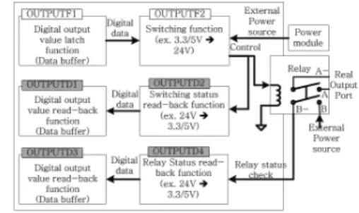
출력 모듈은 CPU module과 인터페이스하기 위한 버스 인터페이스 기능과 수신된 데이터를 저장하기 위한 버퍼 기능, 저장된 데이터를 원하는 출력의 형태 로 변환하여 출력하는 변환 기능 블록으로 구성된다.
또한 내부의 전원을 공급하는 전원 변환 기능을 포함
한다. 출력 변환 기능으로는 출력 전위 변환 기능, 아
날로그 변환기능, 전류 변환 기능, PMW 변환 기능
등이 있을 수 있다. 그림 2는 이러한 기능으로 구성된
출력 모듈의 기본 구조도를 나타낸 것이다. 이러한 기
본 구조도를 바탕으로 분석과정을 통하여 SIL4를 위
한 출력모듈의 구성을 설계하였다. 그림 2에서는 전류
신호 출력과 PWM신호는 정의되어 있으나, 분석 과정
에서는 해당 출력은 제외하였다. 일반적으로 안전 기
능을 수행하는 출력 모듈의 경우, 릴레이나 스위칭 소
자로 구성되기 때문이다. 따라서 본 연구에서는 안전
기능이 릴레이의 출력과 아날로그 출력으로 이루어진
안전 기능으로 가정하였다. CPU module과의 인터페
이스 또한 통신으로도 이루어질 수 있으나, 버스 형태
로 인터페이스 되는 경우로 한정하였다. 단계1은 그림
ID FUNCTION INPUT OUTPUT
OUTP UTF1
Digital output value latch
function
Digital data from local bus
Individual digital bit to Individual
Output (1:output activation,
0:output deactivation)
OUTP UTF2
Switching function
Individual digital bit to control
each Relay (1:output activation (3.3V/5V), 0:output deactivation:(0V))
Individual Relay operation voltage (1:Relay activation
24V, 0: Relay deactivation 0V)
OUTP UTF3
Analog value latch function
Digital data from local bus
Digital byte value to analog
value
OUTP UTF4
Digital to Analog conversion function
Digital byte for converting to
analog value
Analog signal
OUTP UTF9
Voltage conversion
function +5VDC +3.3VDC
OUTP UTF10
Local Bus Interface function
Digital data having meaning from CPU module
Digital data having meaning
ID Failure Mode ID Failure mode
OUTPUTF1
OPF1_FM1 Stuck high(1)
OPF1_FM2 Stuck low(0)
OPF1_FM3 Interruption
OPF1_FM4 Reverse
OUTPUTF2
OPF2_FM1 Stuck high(24v)
OPF2_FM2 Stuck Low(0v)
OPF2_FM3 Interruption
OPF2_FM4 Reverse
OUTPUTF3
OPF3_FM1 Undemanded higher value OPF3_FM2 Undemanded lower value
OPF3_FM3 Fixed value
OPF3_FM4 Fixed 0
OPF3_FM5 Fixed maximum value
OUTPUTF4
OPF4_FM1 Undemanded higher voltage OPF4_FM2 Undemanded lower voltage
OPF4_FM3 Fixed voltage
OPF4_FM4 Interruption
OPF4_FM5 Fixed 0v
OPF4_FM6 Fixed maximum voltage OPF4_FM7 Oscillation voltage
OUTPUTF9
OPF9_FM1 Interruption
OPF9_FM2 Over-voltage(above 3.3VDC) OPF9_FM3 Low-voltage(below 3.3VDC) OPF9_FM4 Oscillation (waveform voltage)
OPF9_FM5 Stuck to ground
OPF9_FM6 Input voltage(5VDC)
OUTPUTF10
OPF10_FM1 Deletion
OPF10_FM2 Corruption
OPF10_FM3 Insertion
OPF10_FM4 Delay
OPF10_FM5 Repetition(fixed)
그림 2. 출력 모듈의 기본 기능 블록도 Fig. 2 Basic functional block diagram for output module
단계2에서는 각 기능 단위에 입출력을 정의하였으 며 그 결과는 표 1과 같다.
표 1. 출력 모듈의 내부 기능 블록의 입출력 정의 Table 1. Input / output definition of internal functional
block for OUTPUT module
단계 3에서는 표 2와 같이 출력 모듈의 내부 기능 블록에 대한 고장 모드를 도출하였다.
표 2. 출력 모듈의 기능 블록에 대한 고장 모드 Table 2. Failure mode to functional blocks of OUTPUT
module
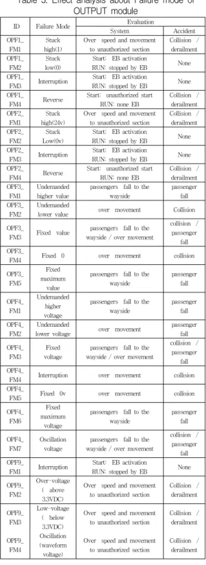
4단계에서는 3단계에서 도출한 각 고장 모드에 대
하여 시스템에 어떤 영향을 초래하는지를 분석하고
평가하였다. 표 3은 이러한 분석의 수행 결과를 보여
준다. 분석 대상으로 선정된 것은 ATP로 열차 신호
시스템 중에서 안전 기능을 수행하는 시스템이다. 분
석을 수행할 때에는 시스템에 대한 최종 상태만 고려
하는 것이 아니라, 각 레벨에 따른 영향을 도출하고,
해당 결과가 상위 레벨의 어떤 상태를 유발시키게 되
는지, 영향의 확산을 분석하여 평가해야 한다[10-12].
ID Failure Mode Evaluation
System Accident
OPF1_
FM1
Stuck high(1)
Over speed and movement to unauthorized section
Collision / derailment OPF1_
FM2
Stuck low(0)
Start: EB activation
RUN: stopped by EB None OPF1_
FM3 Interruption Start: EB activation
RUN: stopped by EB None OPF1_
FM4 Reverse Start: unauthorized start RUN: none EB
Collision / derailment OPF2_
FM1
Stuck high(24v)
Over speed and movement to unauthorized section
Collision / derailment OPF2_
FM2
Stuck Low(0v)
Start: EB activation
RUN: stopped by EB None OPF2_
FM3 Interruption Start: EB activation
RUN: stopped by EB None OPF2_
FM4 Reverse Start: unauthorized start RUN: none EB
Collision / derailment OPF3_
FM1
Undemanded higher value
passengers fall to the wayside
passenger fall OPF3_
FM2
Undemanded
lower value over movement Collision OPF3_
FM3 Fixed value passengers fall to the wayside / over movement
collision / passenger
fall OPF3_
FM4 Fixed 0 over movement collision
OPF3_
FM5
Fixed maximum
value
passengers fall to the wayside
passenger fall
OPF4_
FM1
Undemanded higher voltage
passengers fall to the wayside
passenger fall OPF4_
FM2
Undemanded
lower voltage over movement passenger fall OPF4_
FM3
Fixed voltage
passengers fall to the wayside / over movement
collision / passenger
fall OPF4_
FM4 Interruption over movement collision
OPF4_
FM5 Fixed 0v over movement collision
OPF4_
FM6
Fixed maximum
voltage
passengers fall to the wayside
passenger fall
OPF4_
FM7
Oscillation voltage
passengers fall to the wayside / over movement
collision / passenger
fall OPF9_
FM1 Interruption Start: EB activation
RUN: stopped by EB None OPF9_
FM2
Over-voltage ( above 3.3VDC)
Over speed and movement to unauthorized section
Collision / derailment
OPF9_
FM3
Low-voltage ( below 3.3VDC)
Over speed and movement to unauthorized section
Collision / derailment
OPF9_
FM4
Oscillation
(waveform Over speed and movement to unauthorized section
Collision / derailment
OPF9_
FM5
Stuck to ground
Start: EB activation
RUN: stopped by EB None OPF9_
FM6
Input voltage (5VDC)
Over speed and movement to unauthorized section
Collision / derailment OPF10
_FM1 Deletion Over speed and movement to unauthorized section
Collision / derailment OPF10
_FM2 Corruption Over speed and movement to unauthorized section
Collision / derailment OPF10
_FM3 Insertion Over speed and movement to unauthorized section
Collision / derailment OPF10
_FM4 Delay Over speed and movement to unauthorized section
Collision / derailment OPF10
_FM5
Repetition(fix ed)
Over speed and movement to unauthorized section
Collision / derailment
표 3. 고장 모드에 대한 영향 분석 Table 3. Effect analysis about Failure mode of
OUTPUT module
단계5에서는 단계4에서 도출한 각 고장 모드에 대 한 시스템 영향이 위험을 초래하는 항목에 대해서는 해당 위험이 발생하지 않도록 대비책이 도출되어야 한 다. 즉 해당 고장 모드가 위험을 초래하지 않도록 해 야 하는 것이 요구된다. 이를 위해서는 해당 고장모드 가 발행한 원인을 파악하여, 원인이 발생하지 않도록 하거나, 해당 고장모드가 발생한 상태에서 고장 모드 의 영향이 상위로 확대되는 것을 방지할 수 있는 방안 이 도출되어야 한다. 표 4는 위험을 유발하는 고장모 드에 대한 예방책을 도출한 것이다. 그림 3은 이러한 예방책을 릴레이 출력 포트에 적용한 것이다[13].
표 4. 고장 모드에 대한 예방책
Table 4. Mitigation measures about Failure mode of OUTPUT module
No. Mitigation measures to remove or avoid of cause
1
OUTPUT module periodically sends the status to CPU module to know the failure status(Stuck high, Reverse) of OUTPUTF1/2.
SRAC(Safety Relaed Application Condition) to CPU module : CPU module shall control to the safe status when the failure status of the OUTPUT module is detected.
2
Power status shall be monitored and over-voltage and under-voltage shall be blocked. When the power is recovered, internal power of OUTPUT module can be resupplied.
SRAC to the power supply module: The power supply that supplies the power to the OUTPUT module shall supply the stable voltage.
3
OUTPUT module periodically sends the status to CPU module to know the failure status(Data change) of OUTPUTF3/4.
SRAC to CPU module : CPU module shall control to
the safe status when the failure status of the
OUTPUT module is detected.
그림 3. 릴레이 출력에 대한 예방책 적용 구조도 Fig. 3 Diagram implemented the mitigation measures
for relay output
그림 4. 고장 모드를 검지하기 위한 시험 신호 Fig. 4 Test pulse signal to detect the failure mode
특히 상태가 계속해서 유지되는 출력에 대하여, 해 당 출력이 정상 상태에서의 출력인지, 고장난 상태에 서의 출력인지를 알 수 있어야, 실제 해당 기능이 동 작할 때, 기능이 계속해서 동작됨을 보증 할 수 있기 때문에, 출력 신호에 변화를 주어, 상태를 계속해서 검지할 수 있도록 하였다. 물론 이때에는 최종 출력에 는 영향을 주기 않도록 하였다. 즉 릴레이의 출력에 대하여 아래와 같은 신호를 주기적으로 출력해서 시 험해야 한다. 그림 4(1)은 High 출력을 유지하고 있는 상태에서 출력 제어 회로의 고장을 검지하기 위한 방 안으로 test pulse를 출력하는 것이다. TH의 시간은 Relay의 동작에 영향을 주지 않을 만큼의 시간을 설 정해야 한다. 이 시간은 사용하는 Relay의 특성에 따 라 달라진다. 이렇게 하는 이유는 High 출력 상태에 서 시스템이 안전상태로 가기 위해 출력을 차단할 수 있는지를 계속해서 감시하기 위한 것으로써, 만일 ISO1의 출력이 short된 상태라면, ISO1을 동작시켜 출력을 차단하기 어려운 상태가 된다. 이를 미리 방지 하기 위하여 이러한 시험이 이루어지도록 구성한다.
그림 4(2)는 Low 출력을 유지하고 있는 상태에서 Relay coil의 고장을 검지하기 위한 방안으로 test pulse를 출력하는 것이다. TL의 시간은 Relay가 동작 하지 않을 만큼의 시간을 설정해야 한다. Relay는 동 작하지 않지만, 흐르는 전류를 검지할 수 있도록 구성 되어야 한다. 이러한 설계는 Relay의 상태를 주기적으 로 검사하여 실제 동작시킬 수 있는지를 미리 판단하 기 위함이다. 그림 5는 이렇게 Relay를 시험하기 위한 회로를 구성한 것이다.
그림 5. 릴레이를 시험하기 위한 회로 Fig. 5 Circuit to test the Relay
그림 6은 아날로그 출력기능인 OUTUT3/4에 대하 여 예방책을 적용한 구성도이다.
그림 6. 아날로그 출력에 대한 예방책 적용 구성도 Fig. 6 Diagram implemented the mitigation measures
for analog output
아날로그 신호를 출력하고 있는 상태에서 출력과 관련된 기능인 OUTPUTF3/4의 기능이 정상적인지에 대하여 자체적으로 시험을 수행하기가 어렵다. 이는 출력 신호인 아날로그 신호에 영향을 발생시키지 않 도록 해야 하는 문제점이 있기 때문이다. 따라서 출력 회로에 대한 자체 고장검지는 수행하기 어렵기 때문 에 최종 출력신호의 상태를 감시하는 것으로 대체할 수 있다. 이는 OUTPUTD5/6에 의하여 수행되며, 만 일 출력이 잘못된 상태라고 판단될 때에는 출력 라인 을 차단하여 안전 상태를 유지시키도록 할 수 있다.
여기서 출력을 차단하거나, 출력이 0V인 경우에 외부 장치는 안전상태라는 것을 인식해야 하는 조건이 발 생한다. 이러한 조건은 외부 장치 설계자에게 통보되 도록 해야 한다. 아날로그 출력 신호를 감시하는 회로 동작의 상태가 정상인지를 확인하지 못한다면, 출력 신호에 대하여 보증할 수 없게 된다. 즉 감시기능에 대하여 보증할 수 있어야 한다. 이를 위해서 OUTPUTD7/8 기능을 추가하여 감시 회로의 동작을 주기적으로 감시하도록 구성하였다. 이는 출력에 영향 을 미치지 않으면서, 검사회로를 검사할 수 있는 방안 으로 여겨진다. ISO1부터 ISO3까지는 회로 내부와 외 부를 전기적으로 분리하여, 외부의 영향으로부터 독립 될 수 있도록 구성하여, IEC 62425[1]의 독립성 요구 사항을 만족시키도록 하였다.
그림 7. 출력 모듈의 최종 구성도
Ⅲ. 설계 검증
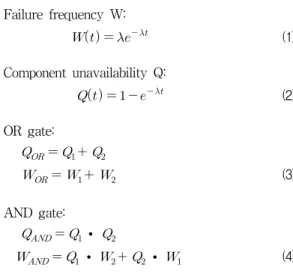
설계에 대한 검증은 고장 계통 분석을 통하여 수행 하였다. 그리고 신뢰성 데이터는 IEC TR 62380[14]을 적용하여 도출하였다. 고장 계통 분석에 대한 결과는 FTA[5]를 이용하여 그림 8과 같이 도출하였다. 10년 일 때의 각 이벤트에 대한 고장빈도와 비가용도는 표 5와 같이 도출되었다.
그림 8. 고장계통분석의 결과 Fig. 8 Fault Tree Analysis result
1단계부터 5단계까지의 분석 과정을 거치면서, 위 험한 고장모드에 대한 대비책의 도출이 완료되었으며, 해당 예방책을 반영하여 그림 7과 같이 최종 구성안 을 도출하였다.
기본 고장율로부터 FTA[5]를 구성하는 상위 이벤
Years Hours Failure Frequency of OUTPUT module (/h)
Failure Frequency of System (/h)
8 70080 1.04636E-08 1.21116E-10
9 78840 1.18323E-08 1.7393E-10
10 87600 1.3215E-08 2.40645E-10
11 96360 1.46121E-08 3.23073E-10
12 105120 1.60238E-08 4.23083E-10
13 113880 1.74501E-08 5.42609E-10
14 122640 1.88914E-08 6.83645E-10
15 131400 2.03479E-08 8.48254E-10
16 140160 2.18198E-08 1.03856E-09
17 148920 2.33072E-08 1.25677E-09
18 157680 2.48105E-08 1.50515E-09
19 166440 2.63299E-08 1.78604E-09
20 175200 2.78655E-08 2.10187E-09
21 183960 2.94177E-08 2.45512E-09
22 192720 3.09867E-08 2.84839E-09
23 201480 3.25727E-08 3.28434E-09
24 210240 3.4176E-08 3.76572E-09
25 219000 3.57968E-08 4.29538E-09
Failure frequency W:
(1)
Component unavailability Q:
(2)
OR gate:
(3)
AND gate:
∙
∙
∙
(4)
표 5. 각 이벤트에 대한 고장빈도와 비가용도의 산출 Table 5. Failure frequency and unavailability for each event
Event ID
Dangerous Failure Rate
(FIT)
W (Failure Frequency)(/h)
Q (Unavailability)
Event Core - 2.41533E-10 5.19326E-06
Event ch1 - 5.2994E-08 0.002278873
Event 4 - 1.32485E-08 0.000569718
Event 41 - 7.8864E-10 2.26424E-05
Event 411 - 4.0466E-07 0.035899437
BEvent 4111 3.134 3.12541E-08 0.002741619
BEvent 4112 4.1253 4.11042E-08 0.003607241
BEvent 4113 34.242 3.32301E-07 0.029550577
Event 412 - 1.48586E-08 0.000630717
Event 4121 - 1.18618E-09 5.20488E-05
Event 41211 - 8.22084E-08 0.007214482
BEvent 412111 4.1253 4.11042E-08 0.003607241
BEvent 412112 4.1253 4.11042E-08 0.003607241
Event 41212 - 8.22084E-08 0.007214482
BEvent 412121 4.1253 4.11042E-08 0.003607241
Bevent 412122 4.1253 4.11042E-08 0.003607241
Event 42 - 2.13711E-10 6.1193E-06
Event 421 - 1.0503E-07 0.009217836
BEvent 4211 4.1253 4.11042E-08 0.003607241
BEvent 4212 5.123 5.10006E-08 0.004477693
BEvent 4213 1.294 1.29253E-08 0.001132902
Event 422 - 1.56204E-08 0.000663854
Event 4221 - 1.9363E-09 8.49685E-05
Event 42211 - 1.0503E-07 0.009217836
BEvent 422111 4.1253 4.11042E-08 0.003607241
BEvent 422112 5.123 5.10006E-08 0.004477693
BEvent 422113 1.294 1.29253E-08 0.001132902
Event 42212 - 1.0503E-07 0.009217836
BEvent 422121 4.1253 4.11042E-08 0.003607241
BEvent 422122 5.123 5.10006E-08 0.004477693
BEvent 422123 1.294 1.29253E-08 0.001132902
Event 43 - 1.22461E-08 0.000540957
Bevent 431 15.285 1.50817E-07 0.013300417
Event 432 - 4.59541E-07 0.040672158
Event 432 - 4.59541E-07 0.040672158
각 년도 별 출력 모듈과 시스템에 대한 고장빈도의 추이가 표 6과 같이 도출되었다. 24년의 시스템의 고 장빈도는 3.76572x10⁻⁹/h로서 목표한 수치와 부합하지 만, 25년부터는 부합하지 않는 것으로 도출되었다.
표 6. 시간에 따른 출력 모듈과 시스템의 고장빈도의 산출
Table 6. Failure frequency for OUTPUT module and system based on time
Ⅳ. 결론
본 연구에서는 안전 관련 시스템이 SIL4 기능을 수
행하기 위해 달성해야 할 정량적 목표인 THR을
4x10⁻⁹/h로 설정한 상태에서 시스템이 입력 모듈, 출
력모듈, CPU모듈, 전원 공급 장치로 구성되었을 때,
출력 모듈에 대하여 목표치를 달성하기 위한 설계 구
조를 제시하였고, 각 내부 구성도의 정량적 목표치의
수준을 정의하였다. 또한 고안된 출력 모듈의 구성 블
록에 대한 회로 설계를 실시하여 FTA를 수행한 결과
10년에의 시스템에 대한 고장빈도가 2.40645x10⁻¹⁰/h
으로 처음 목표로 한 4x10⁻⁹/h보다 작음으로 부합됨
을 알 수 있었다. 또한 출력 모듈에 대해서는 정량적
목표치가 3.57968x10⁻⁸/h이하로 설계되고, composite
fail-safety 구조를 만족한다면, 해당 시스템은 SIL4에
준하는 시스템으로써 평가될 수 있음을 제시하였다.
감사의 글
본 연구는 국토교통부 일반 및 고속철도용 무 선통신 및 제어시스템 실용화사업의 연구비지원 (과제번호15RTRP-B089552-02)에 의해 수행되었 습니다.
References
[1] IEC 62425, “Railway applications- Communication, signaling and processing systems – safety related electronic systems for signaling,”
IEC, Geneva, Switzerland, Sept. 2007.
[2] IEC 61508, “Functional safety of electrical/
electronic/ programmable electronic safety-related systems,” IEC, Geneva, Switzerland, Apr. 2010.
[3] IEC 62061, “Safety of machinery-Functional safety of safety-related electrical, electronic and programmable electronic control systems,” IEC, Geneva, Switzerland, Jan. 2005.
[4] IEC 61511-1, “Functional safety-safety instrumented systems for the process industry sector,” IEC, Geneva, Switzerland, Jan. 2003.
[5] IEC 61025, “Fault tree analysis(FTA),” IEC, Geneva, Switzerland, Dec. 2006.
[6] K. Chung, “Diagnosis of power supply by analysis of chaotic nonlinear dynamics,” J. of the Korea Institute of Electronic Communication Sciences, vol. 9, no. 7, 2014, pp. 753-759.
[7] H. Shin, “Development of constant current SMPS for LED Lighting,” J. of the Korea Institute of Electronic Communication Sciences, vol. 10, no. 1, 2015, pp. 111-116.
[8] Y. Jeong, “A study on control of generators based on SMPS,” J. of the Korea Institute of Electronic Communication Sciences, vol. 7, no. 1, 2012, pp. 107-115.
[9] H. Shin, “Design of LED Driving SMPS for Large Traffic Signal Lamp,” J. of the Korea Institute of Electronic Communication Sciences, vol. 4, no. 2, 2009, pp. 123-129.
[10] Y. Chai, “Development of OPAMP in an A/D Converter for Pressure Measurement,” J. of the Korea Institute of Electronic Communication Sciences, vol. 5, no. 4, 2010, pp. 435-442.
[11] Z. Jin, “A Study on Software Static Analysis Method on IEC 62279,” J. of the Korea Institute
no. 4, 2015, pp. 513-520.
[12] H. Jung, “Study on Precise Positioning using Hybrid Track Circuit system in Metro,” J. of the Korea Institute of Electronic Communication Sciences, vol. 8, no. 3, 2013, pp. 471-477.
[13] S. Ryou, “An Allocation of Safety Integrity Level to Inductive Loop type Train Control System,” J. of the Korea Institute of Electronic Communication Sciences, vol. 8, no. 12, 2013, pp. 1905-1910.
[14] IEC TR 62380, “Reliability data handbook – Universal model for reliability prediction of electronics components, PCBs and equipment,”
IEC, Geneva, Switzerland, 2004.
저자 소개
유등열(Deung-Ryeol Yoo)
2002년 2월 광운대학교 제어계 측학과 졸업(공학사)
※ 관심분야 : 철도제어안전시스템, 제어계측, 자 동화 설비, 반도체 설계, 임베디드 OS
황경환(Kyung-Hwan Hwang)
1981년 8월 연세대학교 전자공 학과 졸업(공학사)
※ 관심분야 : 철도신호, RAMS
이기서(Key-Seo Lee)