• 검색 결과가 없습니다.

Dielectric Properties of Ca<sub>0.8</sub>Sr<sub>1.2</sub>Nb<sub>3</sub>O<sub>10</sub> Nanosheet Thin Film Deposited by the Electrophoretic Deposition Method

N/A
N/A
Protected

Academic year: 2021

Share "Dielectric Properties of Ca<sub>0.8</sub>Sr<sub>1.2</sub>Nb<sub>3</sub>O<sub>10</sub> Nanosheet Thin Film Deposited by the Electrophoretic Deposition Method"

Copied!
5
0
0

로드 중.... (전체 텍스트 보기)

전체 글

(1)

http://dx.doi.org/10.5369/JSST.2018.27.1.1 pISSN 1225-5475/eISSN 2093-7563

Dielectric Properties of Ca 0.8 Sr 1.2 Nb 3 O 10 Nanosheet Thin Film Deposited by the Electrophoretic Deposition Method

Haena Yim

1

, So-Yeon Yoo

1

, and Ji-Won Choi

1,2,+

Abstract

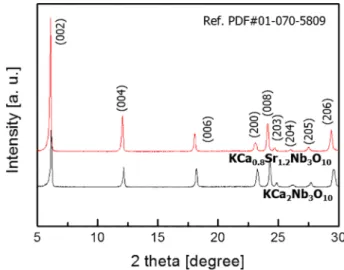
Two-dimensional (2D) niobate-based nanosheets have attracted attention as high-k dielectric materials. We synthesized strontium- substituted calcium niobate (Ca

0.8

Sr

1.2

Nb

3

O

10

) nanosheets by a two-step cation exchange process from KCa

0.8

Sr

1.2

Nb

3

O

10

ceramic. The K

+

ions were exchanged with H

+

ions, and then H

+

ions were exchanged with tetrabutylammonium (TBA

+

) cations. The Ca

0.8

Sr

1.2

Nb

3

O

10

nanosheets were then exfoliated, decreasing the electrostatic interaction between each niobate layer. Furthermore, Ca

2

Nb

3

O

10

nanosheets were synthesized in same process for comparison. Each exfoliated nanosheet shows a single-crystal phase and has a lateral size of over 100 nm. The nanosheets were deposited on a Pt/Ti/SiO

2

/Si substrate by the electrophoretic deposition (EPD) method at 40 V, followed by ultraviolet irradiation of the films in order to remove the remaining TBA

+

ions. The Ca

0.8

Sr

1.2

Nb

3

O

10

thin film exhibited twice the dielectric permittivity (~60) and lower dielectric loss than Ca

2

Nb

3

O

10

thin films.

Keywords: Dielectric, two-dimensional material, niobate, nanosheet

1. INTRODUCTION

The growth of miniaturized electronic devices and nanodevices have encouraged the development of a new class of nanosized materials. In particular, two-dimensional (2D) materials exfoliated from layered perovskite compounds have received attention in recent years for their novel properties, including their electrical, chemical, and optical properties[1]. Among the various 2D materials, the Dion–Jacobson (DJ) layered perovskites have been of interest because of their dielectric and ferroelectric properties in the thin-film region[2]. In case of titanium-based perovskite materials, such as BaTiO

3

, which are typical dielectric materials for various capacitors, the dielectric permittivity is greatly reduced by decreasing the thickness of the film, due to the size effect. On the other hand, the DJ-phase dielectric nanosheets maintain their great dielectric properties, even at thicknesses of a few nanometers[3].

Therefore, many researchers have reported various DJ-phase dielectric nanosheets, such as Ca

2

Nb

3

O

10

(CNO) and Sr

2

Nb

3

O

10

[4,5]. DJ-phase materials consist of a number of BO

6

octahedral slabs and alkali metal A-cations in the formula of A[A’

n-1

B

n

O

3n+1

].

Therefore, we can easily exfoliate each [A’

n-1

B

n

O

3n+1

] perovskite layer by exchanging the cations via a soft-chemical process. Generally, A cations are exchanged for H

+

ions in the acid solution, and then the amine surfactants, such as tetrabutylammonium (TBA

+

), are used to exchange with the H

+

ions. When the large organic TBA

+

ions are intercalated to the perovskite slabs, each negatively charged perovskite layer is naturally delaminated due to swelling[6].

Using these chemically exfoliated nanosheets, thin films can be deposited by a solution-based deposition method, such as electrophoretic deposition (EPD) and layer-by-layer (LBL)[7,8].

However, the LBL method, which requires repetitive positive polyions and negatively charged dielectric layers, takes a long time to deposit a thin film. Whereas, the EPD method, which enable nanosheets to grow a thin film in electric field, is very simple and much faster. In addition, the deposition method can be done in room temperature, so that thin film can be deposited without regard to the kind of substrate including flexible polymer substrate. Because of these advantages, the dielectric nanosheet thin films deposited by the EPD method such as TiO

2

[7] and Ca

2

Nb

3

O

10

[9] have been reported. Also, in order to enhance their dielectric properties, the research on A-site substitution have been

1

Center for Electronic Materials, Korea Institute of Science and Technology, Seongbuk-gu, Seoul 02792, Korea

2

Nanomaterials Science and Engineering, Korea University of Science and Technology, Daejeon 34113, Korea

+

Corresponding author: [email protected]

(Received: Dec. 11, 2017, Revised: Jan. 22, 2018, Accepted: Jan. 23, 2018)

This is an Open Access article distributed under the terms of the Creative Commons Attribution Non-Commercial License(http://creativecommons.org/

licenses/bync/3.0) which permits unrestricted non-commercial use, distribution,

and reproduction in any medium, provided the original work is properly cited.

(2)

investigated. For example, it was reported that the dielectric permittivity of KCa

2

Nb

3

O

10

ceramic is increased as substitution of Sr

2+

ions to Ca

2+

ions because of highly polarized Sr

2+

ions (polarizability of Ca

2+

= 0.471, polarizability of Sr

2+

= 0.863) [10,11].

However, the dielectric properties of strontium-substituted calcium niobate nanosheets have been not investigated so far.

Here, we synthesized Ca

0.8

Sr

1.2

Nb

3

O

10

(CSNO) nanosheets from KCa

0.8

Sr

1.2

Nb

3

O

10

ceramic and deposited thin films on a Pt/Ti/

SiO

2

/Si substrate by EPD method. The structural and dielectric properties of thin films were investigated.

2. EXPERIMENTAL

2.1 Synthesis of CSNO nanosheets

The CSNO nanosheets were prepared by delamination of the layered perovskite compound KCa

0.8

Sr

1.2

Nb

3

O

10

. The starting material was synthesized using a conventional solid-state synthesis method. The parent materials, K

2

CO

3

, CaCO

3

, SrCO

3

, and Nb

2

O

5

, were ground thoroughly by ball milling for 12 h, and the mixture was dried at 100

o

C. The mixture was calcined at 1200

o

C for 10 h in the box furnace. The obtained KCa

0.8

Sr

1.2

Nb

3

O

10

powder was continuously stirred into a 5-M HNO

3

solution at room temperature for 5 days to exchange K

+

ions for H

3

O

+

ions.

After the H

3

O

+

ion- exchanging process, a HCa

0.8

Sr

1.2

Nb

3

O

10

·1.5H

2

O precursor powder was obtained. In order to neutralize the precursor, the ceramic powder was washed with deionized (DI) water. This precursor powder was then dispersed in a tetrabutylammonium hydroxide (TBAOH) solution and continuously shaken at room temperature for 7 days to exfoliate each Ca

0.8

Sr

1.2

Nb

3

O

10

layer. The Ca

2

Nb

3

O

10

nanosheets were prepared in the same way as the comparison material.

2.2 Deposition and analysis of thin films by EPD method

The nanosheet thin films were deposited on a Pt/Ti/ SiO

2

/Si substrate by the EPD method in an acetone medium. An electrical voltage of 40 V was applied for 30 s at room temperature. After deposition of the thin film, ultraviolet irradiation was used to decompose the residual TBA

+

ions. The dielectric properties were measured by an impedance analyzer (4294A, Agilent) with a platinum top electrode deposited by DC sputtering. The crystal structure was observed through X-ray diffraction, and the

microstructure of the thin films was obtained by scanning electron microscope (SEM) images and transmittance electron microscopy (TEM).

3. RESULTS AND DISCUSSIONS

Fig. 1 shows the X-ray diffraction images of the KCa

2

Nb

3

O

10

(KCNO) and KCa

0.8

Sr

1.2

Nb

3

O

10

(KCSNO) starting materials calcined at 1200

o

C. The peaks of the two ceramics were identified in the DJ phase (JCPDS card no. 01-070-5809), indicating that they are well crystallized to a monoclinic unit cell without any secondary phase because of their similar ionic radii (Ca

2+

= 99 pm, Sr

2+

= 112 pm) [12,13]. There is no structural change, except that the peaks were slightly shifted to a lower angle by the substitution of Sr

2+

ions due to the larger ionic size of Sr

2+

ions than of Ca

2+

ions in the lattices.

The microstructure of the KCNO and KCSNO ceramics were investigated by SEM imaging, as shown in Fig. 2 (a) and (b). The grain size of the synthesis powder was over 1 mm, and the lamella structure was clearly presented in both samples.

After synthesizing the starting materials, the intercalated potassium ions were exchanged for protons through acid treatment. Then, proton-intercalated HCa

2

Nb

3

O

10

and HCa

0.8

Sr

1.2

Nb

3

O

10

ceramics were obtained and neutralized by a DI-water washing process. Subsequently, the proton-intercalated ceramics were dispersed in a TBAOH solution and shaken for 7 days. The incorporation of TBA

+

ions into H

+

ions causes expansion of each perovskite layer, as shown in Fig. 3 (a). Finally, Fig. 1. X-ray diffractions of KCa

2

Nb

3

O

10

and KCa

0.8

Sr

1.2

Nb

3

O

10

ceramics.

(3)

the CSNO and CNO (as a comparison material) solution was stabilized by centrifuging at 2000 rpm for 10 min.

The morphological properties of the chemically exfoliated CSNO nanosheets were obtained by TEM observation in Fig. 3 (b), and the lateral size of the CSNO nanosheets were estimated to be over 100 nm. Fig. 3 (c) presents the SEAD pattern of a CSNO nanosheet. It clearly indicates the single-crystal nature of the nanosheet along the [001] direction.

Using the obtained colloidal nanosheets, we deposited a dielectric thin film by EPD on a Pt/Ti/SiO

2

/Si substrate. Fig. 4 (a) and (b) show the top and cross-sectional SEM images of the CNO and CSNO thin films. To grow the thin films, an electrical voltage of 40 V was applied for 30 s. In this condition, the thicknesses of the CNO and CSNO thin films are ~830 nm and ~350 nm, and the uniform and smooth surface thin films can be deposited as shown in the SEM images.

The thickness of the two samples is different under the same deposition conditions because the thickness is dependent on the

concentration of solution. We assume that the different densities of the precursor pellets causes different degrees of cation exchange and concentration. After fabrication of the dielectric thin films, platinum dots were deposited by DC sputtering for a top electrode to measure the dielectric properties.

The dielectric properties of the 830-nm CNO and 350-nm CSNO films are shown in Fig. 5 (a) and (b) according to frequency. The dielectric permittivity (e

r

) of the CNO and CSNO thin films were 32 and 64 at 1 kHz, respectively. The CSNO thin films show twice the dielectric permittivity of the CNO thin film, and this result reflects the properties of the precursor [10]. The Fig. 2. SEM images of (a) KCa

2

Nb

3

O

10

and (b) KCa

0.8

Sr

1.2

Nb

3

O

10

powder.

Fig. 3. (a) A schematic diagram of cation exchange process, (b) TEM image and (c) SEAD pattern of Ca

0.8

Sr

1.2

Nb

3

O

10

nanosheet.

Fig. 4. Top and Cross-sectional SEM images of (a) Ca

2

Nb

3

O

10

thin

film and (b) Ca

0.8

Sr

1.2

Nb

3

O

10

thin film.

(4)

more polarizable Sr

2+

ions increase the dielectric permittivity. As the measuring frequency increased, the both e

r

values slightly decreased to 29 and 52 at 1 MHz. This tendency is caused by the effects of space charge and interfacial polarization from the residual TBA

+

ions. The tand of both thin films were under 0.15 in all frequency ranges. Therefore, the enhanced dielectric thin films can be obtained by simple EPD deposition method by using A-site-substituted CNO nanosheets with Sr

2+

ions, and it can be used as a new material to fabricate dielectric thin films.

4. CONCLUSIONS

We modified the A site of Ca

2

Nb

3

O

10

(CNO) nanosheets to enhance their dielectric permittivity by substitution of more polarizable Sr

2+

ions in the lattice. The Ca

0.8

Sr

1.2

Nb

3

O

10

(CSNO)

colloidal nanosheets were successfully synthesized through two- step cation exchanging process (H

+

ions and TBA

+

ions) from KCa

0.8

Sr

1.2

Nb

3

O

10

ceramic precursor. Synthesized CSNO nanosheets were deposited on a Pt/Ti/SiO

2

/Si substrate as thin film by electrophoretic deposition method, which enables fast and simple deposition. All deposition processes were performed at room temperature. The thickness of the CSNO thin film was about 350 nm, and it exhibited a dielectric permittivity of e

r

= 64 at 1 kHz and 52 at 1 MHz, twice that of CNO.

ACKNOWLEDGMENT

This research was supported by the KIST Future Resource Program (2E27120).

REFERENCES

[1] S. Z. Butler, S. M. Hollen, L. Y. Cao, Y. Cui, J. A. Gupta, H. R. Gutierrez, T. F. Heinz, S. S. Hong, J. X. Huang, A. F.

Ismach, E. Johnston-Halperin, M. Kuno, V. V. Plashnitsa, R.

D. Robinson, R. S. Ruoff, S. Salahuddin, J. Shan, L. Shi, M.

G. Spencer, M. Terrones, W. Windl, and J. E. Goldberger.

“Progress, Challenges, and Opportunities in Two-Dimen- sional Materials Beyond Graphene,” ACS Nano, Vol. 7(4), pp. 2898-2926, 2013.

[2] M. Osada and T. Sasaki. “Two-Dimensional Dielectric Nanosheets: Novel Nanoelectronics From Nanocrystal Building Blocks,” Adv Mater, Vol. 24(2), pp. 210-228, 2012.

[3] M. Osada and T. Sasaki. “New Dielectric Nanomaterials Fabricated from Nanosheet Technique,” ECS Trans., Vol.

45(3), pp. 3-8, 2012.

[4] B. W. Li, M. Osada, Y. Ebina, K. Akatsuka, K. Fukuda, and T. Sasaki. “High Thermal Robustness of Molecularly Thin Perovskite Nanosheets and Implications for Superior Dielectric Properties,” ACS Nano, Vol. 8(6), pp. 5449-5461, 2014.

[5] Y. S. Lee, H. Yim, S. Y. Yoo, B. K. Ju, and J. W. Choi.

“Dielectric properties of single crystal Sr2Nb3O10 dielec- tric nanosheet thin films by electrophoretic deposition (EPD) and post deposition treatments,” J Alloy. Comp., Vol. 711, pp. 51-57, 2017.

[6] F. F. Xu, Y. Ebina, Y. Bando, and T. Sasaki. “Structural characterization of (TBA, H)Ca-2(3)10(Nb)O nanosheets formed by delamination of a precursor-layered perovskite,”

J Phys Chem B, Vol. 107(36), pp. 9638-9645, 2003.

[7] T. Yui, Y. Mori, T. Tsuchino, T. Itoh, T. Hattori, Y.

Fukushima, and K. Takagi. “Synthesis of photofunctional titania nanosheets by electrophoretic deposition,” Chem.

Mater., Vol. 17(1), pp. 206-211, 2005.

[8] T. Sasaki, Y. Ebina, T. Tanaka, M. Harada, M. Watanabe, and G. Decher. “Layer-by-layer assembly of titania Fig. 5. Dielectric properties of (a) Ca

2

Nb

3

O

10

thin film and (b)

Ca

0.8

Sr

1.2

Nb

3

O

10

thin film.

(5)

nanosheet/polycation composite films,” Chem. Mater., Vol.

13(12), pp. 4661-4667, 2001.

[9] S. H. Kweon, M. Im, W. H. Lee, S. Nahm, J. W. Choi, and S. J. Hwang. “Electrophoretic deposition of Ca2Nb3O10- nanosheets synthesized by soft-chemical exfoliation,” J Mater Chem C, Vol. 4(1), pp. 178-184, 2016.

[10] H. Yim, S. Y. Yoo, Y. E. Sung, and J. W. Choi. “Synthesis and dielectric properties of strontium substituted calcium niobate ceramics,” J. Alloy. Comp., Vol. 622, pp. 373-378, 2015.

[11] J. Ying, Nanostructured materials, Elsevier pp. 86, 2001.

[12] C. S. Sun, P. Peng, L. R. Zhu, W. J. Zheng, and Y. N. Zhao.

“Designed reversible alkylamine intercalation-deintercala- tion in the layered perovskite-type oxide KCa2Nb3O10,”

Eur J Inorg Chem, Vol. 24, pp. 3864-3870, 2008.

[13] G. Cho, C.-N. Chau, and J. P. Yesinowski. “

19

F MAS NMR Investigation of Strontium Substitution Sites in Ca

2+

/S

r2

+ Fluorapatite Solid Solutions,” J Phys Chem C, Vol. 112, pp.

6165-6172, 2008.

수치

Fig. 1 shows the X-ray diffraction images of the KCa 2 Nb 3 O 10 (KCNO) and KCa 0.8 Sr 1.2 Nb 3 O 10  (KCSNO) starting materials calcined at 1200 o C
Fig. 4. Top and Cross-sectional SEM images of (a) Ca 2 Nb 3 O 10  thin film and (b) Ca 0.8 Sr 1.2 Nb 3 O 10  thin film.

참조

관련 문서

Second, what effects does the anger-control training have upon sub factors such as physical aggression, verbal aggression, irritability, hostility,

Among the sub-factors of autonomy support coaching behavior, strategy recognition had the most direct influence on the grit of athletes, followed by

Second, as a result of the IPA analysis of the sub-factors of audience perception, the factors of entry route were located in the first quadrant, the

Among the sub-factors, confidence, The factors of setting, team harmony, image and will power were higher in the group with national representative

Third, looking at the sub-factors in terms of textbooks and software by priority, they were in the order of development of textbooks and learning tools

For the gender, while training and direction, democratic direction, positive regard, and autocratic direction of leadership type sub-factors were perceived as high in

For the sub-factors of selection attributes and customer value according to screen golf course handicap, convenience, professionality, facilities, price,

The results of this study are as follows: ⑴ 4 basic directions, 16 themes, and 64 sub-themes of the vocational high school development are established, and