<연구논문>
한국표면공학회지
J. Korean Inst. Surf. Eng
ISSN 1225-8024(Print) Vol.54, No.3, 2021.ISSN 2288-8403(Online) https://doi.org/10.5695/JKISE.2021.54.3.119
1. 서 론
투명전도성 산화물(Transparent Conductive Oxide; TCO) 박막은 높은 가시광 투과율(Visible transmittance, ≥ 80%)과 낮은 면저항(Sheet resistance < 100 Ω/□) 특성을 동시에 갖기 때문에
다양한 표시소자와 박막형 태양전지의 투명전극으로 사용되고 있다[1]. 따라서 상대적으로 우수한 전기광 학적 완성도를 확보하기 위하여 다양한 투명전극 재료 가 개발되었으며, 그 재료 중에서 미량의 주석(Sn)이 첨가된 인듐산화물 (Sn doped In2O3; ITO) 박막이 전자재료 산업 전반에 걸쳐 폭 넓게 활용되고 있다[2].
하지만 최근에는 인듐(In)의 희귀성과 화학적 불안전 성으로 인하여 대체 전극재료를 찾는 연구가 진행되고 있으며 주석(Sn)이 첨가된 Zinc Oxide(ZTO) 박막이 종래의 ITO 박막의 대체 투명전극으로 보고되어, 다
Ag 중간층이 SnO 2 박막의 광학적, 전기적 특성에 미치는 영향
장진규
a
, 김현진a
, 최재욱a
, 이연학a
, 허성보b
, 김유성c
, 공영민a*
, 김대일a*
a울산대학교 첨단소재공학부
b한국생산기술연구원 동남본부 에너지소재부품연구그룹
c한국생산기술연구원 울산본부 첨단정형공정그룹
Influence of Ag Interlayer on the Optical and Electrical Properties of SnO 2 Thin Films
Jin-Kyu Jang
a, Hyun-Jin Kim
a, Jae-Wook Choi
a, Yeon-Hak Lee
a, Sung-Bo Heo
b, Yu-Sung Kim
c, Young-Min Kong
a*, Daeil Kim
a*aSchool of Materials Science and Engineering, University of Ulsan, Ulsan 44776, Korea
bKorea Institute of Industrial Technology, Yangsan 50635, Korea
cKorea Institute of Industrial Technology, Ulsan 44413, Korea
(Received 23 May, 2021 ; revised 27 June, 2021 ; accepted 28 June, 2021)
Abstract
SnO2 single layer and SnO2/Ag/SnO2 (SAS) tri-layered films were deposited on the glass substrate by RF and DC magnetron sputtering at room temperature and then the effect of Ag interlayer on the opto-electrical performance of the films were considered. As deposited SnO2
films show a visible transmittance of 85.5 % and a sheet resistance of 1.2⨉104 Ω/□, the SAS films with a 15 nm thick Ag interlayer show a lower resistance of 18.8 Ω/□ and a visible transmittance of 70.6 %, respectively. The figure of merit based on the optical transmittance and sheet resistance revealed that the Ag interlayer in the SnO2 films enhances the opto-electrical performance without substrate heating or annealing process.
Keywords : SnO
2, Ag, Sheet resistance, XRD, AFM.
*Corresponding Author: Daeil Kim, Young-Min Kong School of Materials Science and Engineering, University of Ulsan
Tel: +82-52-712-8058
E-mail: [email protected], [email protected]
양한 증착공정 연구가 진행되고 있다[3]. 그러나 실온 조건에서 증착된 ZTO 박막은 후속 열처리 없이 투명 전극으로 사용하기에는 높은 비저항을 갖기 때문에 이 를 개선하기 위해 다양한 열 표면처리 기술[4]이 제시 되었으며, Y. Kim과 J, Park 은 gold(Au) 와 nickel (Ni), 등의 금속박막을 사용하여 상온조건에서도 향상 된 전기광학적 특성을 갖는 TCO/metal 이층구조 박 막[5]과 TCO/metal/TCO 삼층구조 박막[6]을 보고 하였다. 본 연구에서는 앞서 ITO/Ag/ITO 적층박막 연구[7]에서 보고된 Ag 박막의 전기광학적 특성 개선 효과를 SnO2박막의 전기광학적 완성도 개선에 적용 하기 위하여, RF와 DC 마그네트론 스퍼터를 이용하여 삼층구조의 SnO2/Ag/SnO2 (SAS) 박막을 증착하고, 실온조건에서 Ag 층간금속의 두께에 따른 광학적, 전 기적 특성 제고 효과를 고찰하였다.
2. 실험방법
본 연구에서는 SnO2 (직경 3 Inch, 순도:
99.95%) 타겟과 Ag(직경 3 Inch, 순도: 99.99%) 타겟이 장착된 RF와 DC 마그네트론 스퍼터를 이 용하여 실온에서 유리기판(3⨉3 cm2)에 SnO2 단 층박막과 SnO2/Ag/SnO2 적층박막 을 증착하였다.
기판은 아세톤, 이소프로판올, 증류수의 순서로 5 분간 초음파 세척을 실시하고 질소가스로 건조하였 으며, 증착조건은 Table. 1에 나타내었다. 증착 후, 단차측정기(Dektak-150, Veeco)을 이용하여 박막의 두께와 증착율을 측정하였고, 기판과 박막 의 가시광 투과율은 자외선–가시광선 분광기 (380-780 nm, Cary 100 Cone, Varian)로 분석 하였으며, 기판의 가시광 투과율은 93.0% 이었다.
층간 Ag 박막의 두께변화에 따른 결정성은 X선 회 절분석기 (X-ray diffraction Xpert -APD, Philips, Cu-Kα radiation λ= 0.154 nm, 기초 과학지원연구원, KBSI 대구센터)로 분석하고, 표면 조도(Root mean square roughness, RMS 거칠 기)는 원자간력현미경(Scan area 2×2 μm2, XE-100, Park system)으로 측정하였다. 박막의 면저항(Sheet resistance)은 Four point probe (HMS-3000, Ecopia)로 측정하였으며, 박막의 Figure of merit[8] 수치로 전기광학적 완성도 (Opto-electrical performance)를 평가하였다.
Base pressure (Torr) 7.0 × 10
-7Deposition pressure (Torr) 1.0 × 10
-3SnO
2RF Power (W/cm²) 3.0
Ag DC Power (W/cm²) 2.0
Ar gas flow rate (sccm) 10.0 Thickness (nm)
SnO
2single layer SnO
2/Ag/SnO
2tri-layer
30/10/30, 30/15/30, 60 30/20/30 Deposition rate (nm/min)
SnO
2/Ag 15 / 40
Table 1. Experimental condition of SnO
2and SnO
2/Ag/SnO
2tri-layer deposition.
3. 결과 및 고찰
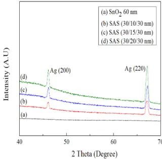
Fig. 1은 SnO2 단층박막과 층간 Ag 박막 두께에 따른 SAS 적층박막의 X선 회절분석 결과이다. Ag 박막의 두께가 증가할수록 Ag(200) 및 (220)면의 결정립 크기가 미약하게 증가하여 결정성이 향상되 는 경향을 알 수 있으며, SnO2 박막은 비정질구조 로서 층간 Ag 박막의 두께변화에 따른 영향을 받 지 않았다. Table 2에 아래의 Scherrer 관계식[3]
으로 구한 결정립의 크기(D)를 나타내었다.
D = 0.9
λ
/ B Cos θ (1)수식에서 D는 결정립 크기, λ는 X선의 파장 0.154 nm, B는 반치폭 (Full width at half maximum, FWHM), θ는 Bragg 회절각도를 의미 한다.
Fig 1. XRD pattern of the SnO
2single layer and
SnO
2/Ag/SnO
2(SAS) tri-layer films.
Thickness
(nm) Ag 2 Theta
(Deg.) FWHM
(Deg.) Grain size (nm)
SnO2 - - - Amorphousness
30/10/30 (200)
46.09 0.358 24.1
30/15/30 46.08 0.356 24.3
30/20/30 46.07 0.328 26.3
30/10/30 (220)
67.11 0.430 22.2
30/15/30 67.10 0.425 22.5
30/20/30 67.08 0.414 23.1
Table 2. Grain size of Ag interlayer on the SnO
2/Ag/SnO
2(SAS) films.
SAS 박막의 표면거칠기는 전기광학적 완성도에 영향을 미치므로 전극재료의 활용도를 평가할 수 있는 중요한 요소이다. Fig. 2에 원자간력현미경을 이용한 SnO2 와 SAS 박막의 표면형상과 RMS 거 칠기를 나타내었다. SnO2 박막의 거칠기는 1.25 nm 이었으며, 10 nm 두께의 Ag 층간박막을 적 용한 SAS 박막의 거칠기는 1.17 nm로서 미세하 게 감소하였고, 15 nm 두께의 Ag 층간박막을 적 용한 SAS 박막의 거칠기는 1.15 nm로 감소하였 다. 이러한 RMS 거칠기 감소는 Fig. 1과 Table 2 로부터, 10 nm 두께의 Ag 층간막에서 단일층 성 막(One layer formation)으로 표면평탄화가 향상 되었으며, Ag 박막의 두께 20 nm 조건에서 다시 증가된 거칠기(1.20 nm)는 Ag 층간박막의 결정성 향상으로 사료된다 [9].
Fig 2. Surface morphology and RMS roughness of the SnO
2single layer and SnO
2/Ag/SnO
2tri-layer films.
(a) SnO
260 nm; 1.25 nm, (b) SnO
230/Ag 10/SnO
230 nm; 1.17 nm, (c) SnO
230/Ag 15/SnO
230 nm; 1.15 nm, (d) SnO
230/Ag 20/SnO
230 nm; 1.20 nm.
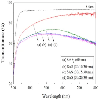
Fig. 3에 SnO2 와 SAS 박막의 가시광 투과도를 나타내었다. SnO2 박막의 가시광 투과도는 85.5%, Ag 10 nm 박막을 적용한 SAS 박막의 가시광 투 과도는 67.3%로 감소함을 보였으나, Ag 15 nm 박막을 적용한 SAS 박막의 투과도는 70.6%로 증 가함을 보였다. 적정 두께의 Ag 박막 적용에 의한 가시광 투과도 제고 현상은 Y. J. Park[9]과 Y. J.
Lee[10]의 연구결과와 같은 층간박막의 거울효과 (Mirror effect)와 상부 SnO2 박막의 반사방지 효 과로 판단되며, Ag 20 nm 박막을 적용한 SAS 박막의 가시광 투과도(66.2%) 감소는 상대적으로 후막화된 금속 층의 광 흡수율 증가로 사료된다.
Fig 3. Optical transmittance of the SnO
2single layer and SnO
2/Ag/SnO
2(SAS) tri-layer films.
Table 3에 SnO2와 SAS 박막의 Figure of merit(FOM) 변화를 나타내었다. FOM 수치는 투 명전도성 소재의 전기적, 광학적 완성도를 비교할 수 있는 기준으로서, 가시광 투과율과 전기전도도 는 서로 반비례 관계를 가지며 관계식(2)은 아래와 같다.
FOM = T10/ Rsh (2)
위 관계식에서 T는 가시광 투과율이며 Rsh는 박막 의 면저항을 의미한다. 본 연구에서 SnO2 박막의 FOM 수치는 1.75×10⁻⁵ Ω−1, SnO2 30/Ag 15/SnO2 30 nm 박막은 층간 Ag층의 단일층 성 막 효과로 인하여 면저항(18.8 Ω/□)의 급격한 감 소를 보이며, SnO2 박막 보다 높은 1.63×10⁻³ Ω
−1 의 FOM 수치를 보였다. SnO2 박막 보다 15 nm 두께의 Ag 박막이 삽입된 SAS 박막이 높은
FOM 수치를 보임으로써, 적정 두께의 Ag 박막을 적용한 SAS 박막이 전기광학적 특성 제고에 효과 적인 구조임을 알 수 있었다.
Thickness Sheet resistance
[Ω/□]
Visible Transmittance
[%]
FOM [Ω-1]
SnO2 60 12 ⨉ 104 85.5 1.75 ⨉
10-5
SAS
30/10/30 40.6 67.3 4.73 ⨉
10-4
30/15/30 18.8 70.6 1.63 ⨉
10-3
30/20/30 11.6 66.2 1.39 ⨉
10-3
Table 3. Figure of merit (FOM) of SnO
2and SnO2/Ag/SnO2 (SAS) thin films.
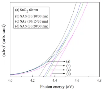
Fig. 4에 SnO2와 SAS 박막의 광학적 밴드-갭 (Optical band-gap)과 흡수계수(αhν)2의 관계를 나타내었다. 광학적 밴드-갭을 구하는데 필요한 박 막의 흡수계수는 아래 관계식으로 나타낼 수 있다 [11].
α = (1/t) ln(1/T) (3)
관계식(3)에서 α는 흡수계수, t는 박막의 두께, T 는 평균 가시광 투과율을 뜻하며, 흡수계수와 광학 적 밴드-갭의 관계는 다음과 같다[12].
(αhν)2 = hν-Eg (4)
관계식(4)에서, h는 Planck 상수, ν는 광자 (Photon)의 진동수, Eg는 광학적 밴드-갭을 의미 한다. Fig. 4에서 SnO2 단층박막의 광학적 밴드- 갭은 4.257 eV, SAS 적층박막의 광학적 밴드-갭 은 Ag 박막의 두께에 비례하며 4.309, 4.329, 4.354 eV까지 증가하였다. Fig. 4의 광학적 밴드- 갭 증가는 앞서 보고된 Y. Song의 ZTO/Ag/ZTO 박막의 광학적 밴드-갭 측정 연구[13]와 유사한 결 과로서, Ag 층간금속 두께 증가에 따른 박막의 전 하밀도 증가 현상으로 사료된다.
Fig 4. Optical band gap of the SnO
2single layer and SnO
2/Ag/SnO
2(SAS) tri-layer films.
4. 결 론
본 연구에서는 RF와 DC 마그네트론 스퍼터를 이용하여 실온조건에서 유리기판에 SnO2 단층박막 과 SnO2/Ag/SnO2 적층박막을 증착하고, Ag 층간 박막 두께에 따른 전기적, 광학적 특성 변화를 고 찰하였다. X선 회절분석을 통하여 Ag 10 nm 두 께부터 Ag 박막의 성막화가 진행된 것을 알 수 있 었으며, 15 nm 두께의 Ag 금속층 조건에서 1.15 nm의 최소 RMS 거칠기가 측정되었다. 또한 층간 Ag 박막의 두께에 반비례하여 면저항이 감소하였 으며 SnO2 30 nm/Ag 15 nm/SnO2 30 nm 적 층박막이 SnO2 단층박막보다 우수한 성능지수 (Figure of merit)를 나타내어 경량성과 유연성을 갖는 표시소자용 투명전극 재료임을 알 수 있었다.
후 기
이 논문은 2021년도 정부(교육부)의 재원으로 한국연구재단의 지원을 받아 수행된 기초연구사업 임(2018R1D1A1B07051003).
References
[1] D. Kim, Improved electrical and optical properties of GZO films with a thin TiO2
buffer layer deposited by RF magnetron
sputtering, Ceram. Inter., 40 (2014) 1457-1460.
[2] D. Kim, Low temperature deposition of ITO on organic films by using negative ion assisted dual magnetron sputtering system, vacuum., 81 (2006) 279-282.
[3] T. K. Gong, S. B. Heo, D. Kim, Effect of postdeposition annealing on the structural, optical and electrical properties of ZTO/Ag/ZTO trilayered films, Ceram.
Inter., 42 (2016) 12341-12344.
[4] M. B. Ali, A. Addad, S. M. Alshahrani, H. A.
S. Al-Shamiri, B. Elgammal, H. Elhouichet, Processing and physical properties of nanomaterials based Zn-Sn-O elements at various annealing temperatures, Optik., 203 (2020) 164005.
[5] Y. S. Kim, J. H. Park, D. Kim, Influence of Au underlayer thickness on the electro-optical properties of ITO/Au layered films deposited by magnetron sputtering on unheated polycarbonate substrates, Vacuum., 82 (2008) 574-578.
[6] J. H. Park, J. H. Chae, D. Kim, Influence of nickel thickness on the properties of ITO/Ni/ITO thin films, J. alloys compd., 478 (2009) 330-333.
[7] S. Y. Lee, Y. S. Park, T. Y. Seong, Optimized ITO/Ag/ITO multilayers as a current spreading layer to enhance the light output
of ultraviolet light-emitting diodes, J. alloys compd., 776 (2019) 960-964.
[8] G. Haacke, New figure of merit for transparent conductors, J. Appl. Phys., 47 (1976) 4086-4089.
[9] Y. J. Park, S. H. Choe, Y. S. Kim, B. C. Cha, Y. M. Gong, D. Kim, Influence of Au Interlayer Thickness on the Opto-Electrical Properties of ZnO Thin Films, . Korean Inst.
Surf. Eng., 53 (2020) 104-108.
[10] Y. J. Lee, D. S. Rub y, D. W. Peters, B. B.
McKenzie, J. W. P. Hsu, ZnO Nanostructures as Efficient Antireflection Layers in Solar Cells, Nano Letters., 8 (2008) 1501-1505.
[11] S. Peng, T. Yao, Y. Yang, K. Zhang, J. Jiang, K. Jin, G. Li, X. Cao, G. Xu, Y. Wang, Influences of the RF power ratio on the optical and electrical properties of GZO thin films by DC copled RF magnetron sputtering at room temperature, Physica B., 503 (2016) 111-116.
[12] J. Tauc, Amorphous and liquid semiconductor, Plenum, New York (1974).
[13] Y. H. Song, T. Y. Eom, S. B. Heo, D. Kim, Effect of Post-deposition Rapid Thermal Annealing on the Electrical and Optical Properties of ZTO/Ag/ZTO Tri-layer Thin Films, J. Korean. Soc. Heat Treat. 30 (2017) 151-154.