Journal of Navigation and Port Research International Edition Vol.36, No.9 pp. 737~740, 2012 (pISSN-1598-5725/eISSN-2093-8470) DOI : http://dx.doi.org/10.5394/KINPR.2012.36.9.737
- 737 -
A Miniaturized CMOS MMIC Bandpass Filter with Stable Center Frequency for 2GHz Application
†In Ho Kang, Xin Guan*
†Dept. of Radio Engineering, Korea Maritime University, Busan, Korea
*Dept. of Radio Engineering, Korea Maritime University, Busan, Korea
Abstract : A miniaturized CMOS bandpass filter for a single RF transceiver system is presented, using diagonally end-shorted coupled lines and lumped capacitors. In contrast to conventional miniaturized coupled line filters, it is proven that the effective permittivity variation of the coupled transmission line has no effect on shifting the center frequency when the bandpass filter is highly miniaturized.
A bandpass filter at a center frequency of 2 GHz was fabricated by 0.18 µm CMOS technology. The insertion loss with the die area of 1500 µm × 1000 µm is -5.14 dB. Simulated results are well agreed with the measurements. It also verify the center frequency stability in the compact size bandpass filter.
Key words : stable center frequency, effective permittivity, coplanar coupled line, miniaturized bandpass filter, CMOS technology
†Corresponding author, [email protected] 051)410-4422
* [email protected] 051)410-4919
1. Introduction
Bandpass filters (BPF) in the frequency band from 2 to 5 GHz in the modern mobile wireless communication systems are usually off-chip surface acoustic wave (SAW) or low temperature ceramic co-fired (LTCC) filter. Recently, CMOS BPFs for a single RF transceiver chip have been developed, driven by reduced costs and decreased RF system design times. In conventional miniaturized coupled line filters with step impedance resonators (SIR) (Makimoto, 1980), the center frequency is shifted when a filter substrate’s effective permittivity is changed. This means that the center frequency is varied when the integrated filter is packaged or mounted onto a circuit board. It is inherently difficult to tune out this frequency variation within the integrated circuit environment.
In this paper, this problem will be addressed by using highly miniaturized BPFs fabricated using the CMOS process. The center frequency of an integrated BPF will be mathematically proven to be stable no matter how it is packaged, when it is highly miniaturized. This will also be confirmed by both electromagnetic simulation and measurement.
2. CMOS integrated bandpass filter
2.1 Conventional SIR Bandpass Filter
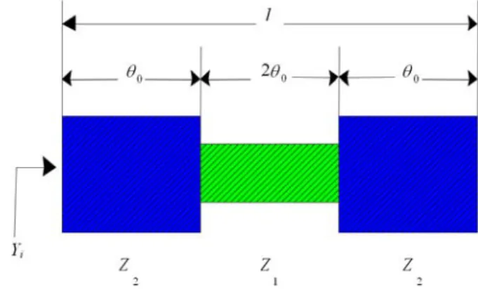
A traditional compact SIR BPF has been shown in Fig. 1,
Fig. 1 Basic structure of a conventional, stepped-impedance resonator
consisting of two types of transmission lines with characteristic impedances of Z1 and Z2. l and θ0are the physical and electrical lengths, respectively. Referring to Fig. 1, the resonance condition is obtained by taking Yi=0, thus giving:
2 ) tan(
tan2
1
2 l
Z Z
eff o
o= ×
= θ λπ ε
(1) Here, εeff is the effective permittivity and λ0 is the free-space wavelength at the resonance frequency. Since coplanar waveguide is usually used in the CMOS process, the characteristic impedance of coplanar waveguide is given by (Wadell, 1991).
A Miniaturized CMOS MMIC Bandpass Filter with Stable Center Frequency for 2GHz Application
- 738 - )
( ) ' ( 0 . 30
, t
t t eff
o K k
k Z K
ε
= π (2)
where K is a constant which is determined by cross-sectional geometry of the waveguide. When εeff
changes, the left hand side of (1) does not change because εeff is cancelled in the numerator and denominator. It can be seen from the right hand side of (1) that the center frequency will shift as εeff changes.
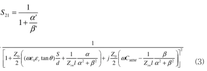
2.2 Highly Miniaturized CMOS Bandpass Filter In contrast, consider now a highly miniaturized coupled line BPF with a short electrical length. When the even and odd impedance of the coupled lines are nearly the same, BPF miniaturization can be realized (Kang, 2007a). Fig. 2(a) shows a highly miniaturized coupled line BPF and Fig. 2(b) is its equivalent circuit and the value of S21 can be given by
' 1 '
1
21
β +α
= S
2
2 2 0
2 0 2
0 1
2 ) 1
tan 2 (
1
1
⎥⎥
⎦
⎤
⎢⎢
⎣
⎡ ⎟⎟⎠
⎜⎜ ⎞
⎝
⎛
− +
⎟⎟+
⎠
⎜⎜ ⎞
⎝
⎛
+ + +
⋅
β α ω β
β α θ α ε
ωε Z C Z l
l j Z d S Z
oe MIM oe
r (3)
where α and β are the attenuation and propagation constant of even mode coupled line. α' and β’ are attenuation and propagation constant in the miniaturized line with the characteristic impedance of Z in Fig. 2(b).
Here, the focus we interested in (3) is the imaginary part of the denominator. The resonance condition is satisfied if the imaginary part is zero, and this section also decides the center frequency of a BPF.
The attenuation constant is composed of conductive loss and dielectric loss. This in the coplanar coupled line can be expressed as (Gopinath, 1982), (Ghione, 1997)
) ' ' ( ) ( 480
) 1
( 2
K K K
k R
e e
ac eff s
ce π β β
α = ε −
(4)
g eff r d
q λ
ε δ
α = ε tan
(5) The propagation constant can be shown as
εr
ε μ ω
β= 0 0 (6)
The value of the square of α in the denominator of the
imaginary part in (3) can be ignored as it is too small compared with β. The decision condition of center
frequency can be simply expressed by
1 0
1 =
− β
ωC Z l
oe
MIM (7) And even-mode impedance of coplanar coupled line can be expressed as [5]
) (
) ( 60
e e eff
oe K
Z K
ββ ε
π ′
= (8) where K’ is a constant to be related to geometrical cross-section. So that in (8), if we assume the thickness of substrate is very thick, the following is satisfied
2 / ) 1 ( r
eff ε
ε ≈ + (9) Since the permittivity of Si substrate is 11.9, εeff is nearly equal to εr/2. In this case, εeff in (7) can be canceled.
It can be proven that when the value of εr varies, the center frequency in (7) will be stable. This means when the chip using RF-CMOS process is being packaged, no matter what is the relative permittivity of the package, it will not cause the changes of frequency characteristics, which can be a great merit for designers and manufacturers. In order to confirm the same situation with the frequency stability of miniaturized BPF above, we fabricated an RF-CMOS chip with the die area of 1500μm × 1000μm.
θ
Z C
C
(a)
v l l
p
β ω θ= =
oe p
o e vC
Z 1
= θ Z
Zoe θ
C C
(b)
Fig. 2 (a) A miniaturized coupled line BPF with short electrical length and (b) its equivalent circuit
In Ho Kang, Xin Guan
- 739 - 3. Simulations and measurements
3.1 Simulated Results
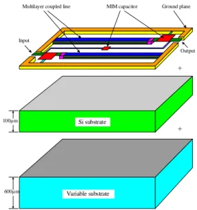
In order to support (7), BPF circuits with different substrates have been simulated using HFSS. Fig. 3 shows the structure of the BPF. In this circuit, the value of the loading capacitance is 3.72 pF and the electrical length θ is 6.49°. The even and odd mode impedances are 195.2Ω and 96.3Ω, respectively. In the metal layers, the slot of coupled line in coplanar coupled line is 250 μm and the distance from the coupled line to ground is 315μm. The width of the coupled line is 25 μm. The HFSS simulated results of the BPF with different substrates are plotted in Fig. 4. Four different kinds of substrate configurations are used. The black line shows the result of the model with a composite substrate which is composed of silicon (Si, of relative permittivity 11.9) and a bottom ceramic layer of relative permittivity 5.8, of thicknesses 100 μm and 600 μm, respectively; the red line is for the same Si with a bottom layer of relative permittivity 36; the blue line is for Si with a bottom layer of air the green line is for the Si substrate connected directly to a bottom ground conductor. The center frequency can easily be shown not to change when the relative permittivity of the bottom dielectric layer shown in Fig. 3 changes. The simulated results are agreed well with the behavior predicted from (7). The overall conclusion is that the dielectric materials under the substrate and the package of the integrated BPF have very little effect on its center frequency when it is highly miniaturized BPF.
100µm
600µm
+
+
Variable substrate Si substrate Input
Output Multilayer coupled line MIM capacitor Ground plane
Fig. 3 The structure of the BPF with different substrates
Fig. 4 The simulated results of the BPF with different substrates by HFSS
3.2 Measurement Results
The die micrograph in Fig. 5 shows a fabricated integrated BPF with pads, with total die area (including the capsulated ground plane) of 1500 µm × 1000 µm. It was manufactured by the Magna chip 0.18 µm CMOS process.
The measured results of this BPF are plotted in Fig. 6. The different colour of each line has the same meaning in Fig.4.
Its insertion loss of 100µm Si substrate situation is about -5.14 dB with return loss of -29.7 dB. Though the insertion loss of -5.14 dB is too lossy, this approach had one of best quality factors in the CMOS process (Kang, 2009b)
The simulated result shows an excellent wideband agreement with the measured result.
The characteristic curve under the situation when the relative permittivities are 5.8 and 36, respectively, which are the ceramic materials fabricated from LTCC, agreed well with the presumption in (7), as the difference of relative permittivity will not cause the change of center frequency.
Nevertheless, when the bottom of 100 µm substrate connects directly to the ground, center frequency moves to the right. This fact supports that material which is under substrate height of 100 µm still has an effect on the characteristic of miniaturized coupled line filter.
Fig. 5 A die micrograph of the integrated BPF
A Miniaturized CMOS MMIC Bandpass Filter with Stable Center Frequency for 2GHz Application
- 740 - Fig. 6 The measurement results of the BPF with different
substrates
4. Conclusion
A MMIC BPFfor a single RF transceiver system at 2.0 GHz was realized using the 0.18 μm CMOS process with chip size of 1500 μm × 1000 μm. In contrast to a conventional SIR filter, it was proven to have a relatively stable center frequency with respect to changes in the permittivity of substrate and filter package. The simulated results agreed well with those measured. The stable center frequency demonstrated for this miniaturized BPF is a highly advantageous feature when embedding it into the transceiver chip.
Acknowledgements
Followings are supported by Basic Science Research Program through the National Research Foundation of Korea (NRF) funded by the Ministry of Education, Science and Technology (2010-0024343).
References
[1] Gopinath A.(1982), "Losses in Coplanar Waveguides,"
IEEE Transactions on Microwave Theory and Techniques, Vol. MTT-30, No. 7, July, pp. 1101-1104.
[2] Ghione, G., Goano, M.(1997), "A Closed-Form CAD- Oriented Model for the High-Frequency Conductor Attenuation of Symmetrical Coupled Coplanar Waveguides," IEEE Transactions on Microwave Theory and Techniques, Vol. 45, No. 7, July, pp. 1065-1070.
[3] Kang, I., Shan, S., Wang, X., Yun, Y., Kim, J., Park, C.(2007a), "A Miniaturized GaAs MMIC filter for the
5GHz band," Microwave Journal, Vol. 50, Nov. 2007, pp.
88-94.
[4] Kang, I., Zhang, H., Yun, Y., Tasker, P., Benedikt, J., Porch, A.(2009b), "High Quality Factor Extraction of Miniaturized Coupled Line Bandpass Filters Implemented Using RF Silicon Integrated Circuits,"
EuMC, pp. 1169.
[5] Makimoto, M., Yamashita, S.(1980), "Bandpass filters using parallel coupled strip-line stepped impedance resonators," IEEE Trans, Microwave Tech., Vol.
MTT-28, No. 12, Dec, pp. 1413-1417.
[6] Wadel B.(1991), Transmission Line Design Handbook, Artech House.
Received 18 September 2012 Revised 24 December 2012 Accepted 26 December 2012