DOI : 10.5394/KINPR.2010.34.7.543
Modified Compact Combline Filter Using Planar Parallel Coupled Structure with Extended Rejection Bandwidth
In-Ho Kang*․Kai Wang**․Shang MIng Li***
*,**,*** Dept. of Radio Engineering Korea Maritime University
Abstract : Modified compact combline bandpass filters are proposed based on the miniaturized quarter-wave transmission line which is composed of the parallel coupled line and lumped capacitors. The electrical length of the parallel coupled line in a resonator, which determines the size of combline bandpass filters, is just 5°or 7°, resulting in a compact circuit area. The designed combline bandpass filter also has a wide upper stopband by suppressing the spurious passbands, not moving. Measured results of two fabricated filters centered at 400MHz show good agreement with the theoretical predications.
Key words : Miniaturization; combline filter; parallel coupled line
* [email protected], 051)410-4422 ** [email protected], 051)410-4919
*** [email protected], 051)410-4919
1. Introduction
Microwave bandpass filters with compact size and low cost are intensely required in modern mobile wireless communication systems because miniaturization is in great demand for most mobile platforms. The parallel coupled line filter proposed by Cohn (1958)has been widely used in microwave systems over the last decades due to its planar structure, simple synthesis procedures and fabrication facility.
Nevertheless, these conventional parallel coupled line filters are too large to apply to mobile communication systems. To reduce the size, folded hairpin resonator filters(Hong, 1998;
Sagawa, 1989;Djaiz, 2006)and stepped-impedance filters were developed (Makimoto, 1980;Kuo, 2003;Wang, 2004;
Kong, 2004), and slow wave open-loop resonator filters have been investigated(Hong, 1997;Hong, 1996;Piston, 2006).
Using the above proposed methods, compact bandpass filter can be achieved. However, they still take up quite a large circuit area, especially at lower microwave frequency band.
Another disadvantage of the traditional parallel coupled line filters is that the first spurious passband of this type of filter appears at twice of the basic passband frequency (2 ), which may seriously degrade the attenuation level in the stopband and passband response symmetry. This is because the phase velocity of the even mode is always slower than that of the odd mode due to the inhomogeneous medium of microstrip structure. The unequal modal phase velocities at 2 cause the first spurious
passband and this could limit the applicability of the filter.
Many papers have been proposed to overcome this problem.
To compensate slow even mode velocity, the parallel coupled line filters with over coupled line stages is proposed to extend the electrical length of odd mode (Kuo, 2003). A proper height of substrate suspension can be used to equalize the even- and odd-mode phase velocities in the parallel coupled line filters(Kuo, 2004). In wiggly-line filter structure, wave impedance using the continuous perturbation of the width of the coupled line can be modulated so that the harmonic passband is rejected(Lopetegi, 2001). Meandered parallel coupled line filters also effectively suppress the spurious passband(Wang, 2005). However, the first spurious passband of these published filters is just moved to the higher frequency, and not removed. The upper spurious passbands still exist in these filters.
Combline filters using low temperature co-fired ceramic (LTCC) or the ceramic material with the feature of three dimensional structures can be used as reduced size bandpass filters(Tang, 2003;Tang, 2006;Yao, 1996).
Conventionally, the electrical length of combline filters has been recommended as 45º or less for efficient coupling (Matthaei, 1980). Moreover, it is not straightforward to calculate the self- and mutual-capacitances for the combline filter with lumped components, and an accurate analysis of the combline structure is a required procedure.
The modified comb-line filter with the electrical length of
10º was published (Wang, 2009). This paper was focused on the harmonics suppression for the power amplifier efficiency improvement, not highly miniaturizing the filter.
For the compact size design, the bandpass filter with lumped elements also can be a solution. But this lumped-element approach is somewhat empirical and has been confined to frequencies up to a few GHz due to the low quality factor and low resonant frequencies(Ju, 1984).
In this paper, a new method will be introduced to miniaturize the size of bandpass filters to as small as a few degrees. There is no spurious in this structure. For the simple fabrication, modified combline filter with the planar microstrip structure will be used.
This paper is organized as follows: In section 2, the limitations of the conventional stepped-impedance resonator will be introduced. Then miniaturized quarter-wave transmission line is introduced in section 3, which plays a key role in building the proposed bandpass filter. Following section 3 is the design method of the bandpass filter in Section 4. To get better performance some tunings are needed before fabrication and this is discussed in Section 5.
Also presented in section 5 is the measured results of two fabricated bandpass filters centered at 400MHz. Conclusions are in section 6.
2. Limitations of Stepped-Impedance Resonator Filters
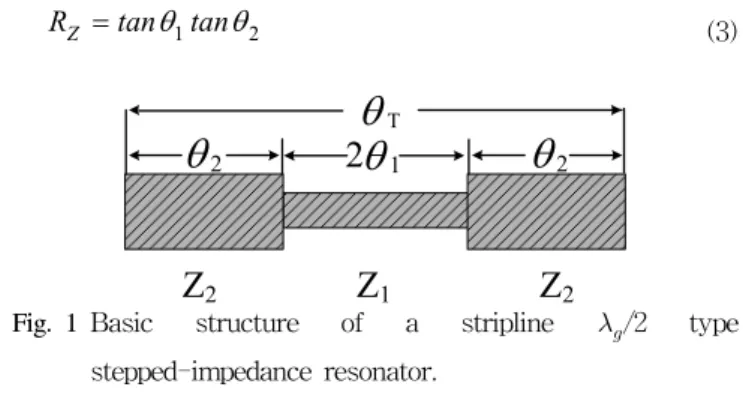
Stepped-impedance resonator bandpass filter has been studied for a compact size. Fig. 1 gives the basic structure of half-wave stepped-impedance resonator filters. It consists of two kinds of transmission lines with the characteristic impedances being and . The high-impedance lines act as series inductors, while the low- impedance lines act as shunt capacitors. The input admittance seen from an open-end is(Makimoto, 1980):
2
1 2 1 2
1 2 1 2
2 2 2
2
1 1 2 1
Z Z
Z Z
Y i jY .
( R tan tan )( R -tan tan ) R ( -tan )( -tan )- ( R )tan tan
θ θ θ θ
θ θ θ θ
=
+
+ (1)
where the impedance ratio is defined by
1 2
Z R Z = Z
(2) Resonance condition is obtained by taking , thus giving:
1 2
R Z = tan θ tan θ (3)
Z 2 Z 1 Z 2
θ T
θ 1
θ 2 2 θ 2
Fig. 1 Basic structure of a stripline /2 type stepped-impedance resonator.
The relationship between the total electrical length of the resonator and , is given by
T 1 2
1
1 1
2
2 1
)
Z Z
(
R ( tan ( tan θ )),R θ θ θ
θ
+
−
=
= + ≠ (4)
From (4), it can be shown that to obtain the smallest filter size, we should choose a very small value of . This can be done by decreasing and increasing . However, if becomes very large, it is very difficult to fabricate the circuit. Therefore, stepped-impedance resonator filters have limitations in size-reduction.
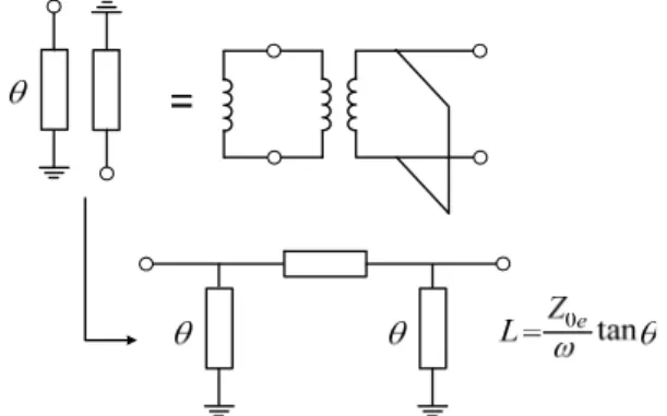
3. Miniaturization of Quarter-Wave Transmission Line
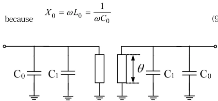
Before starting our filter design theory, the size-reduction method of a λ/4 transmission line will be briefly introduced here(Kang, 2003). As is well known, the line can be replaced with a lumped circuit, as given in Fig. 2, and the value of C 1 is given by
1 0
C 1 ω Z
= (5)
where Z 0 is the characteristic impedance of the quarter-wave transmission line and the angular frequency.
Fig. 2 The equivalent lumped circuit of the quarter-wave
transmission line.
Now to replace the lumped inductor, we add two artificial LC resonators consisting of C 0 and L 0 at each side of the lumped inductor, and then we can get Fig. 3. The dotted network in Fig. 3 is equal to the circuits in Fig. 4 (a) and (b) when (6) and (7) are satisfied.
0 0e
X = Z tan θ (6)
0 0
0 0
2 e o
L
e o
X Z Z tan
Z Z θ
= − (7)
where , = even and odd mode impedances of the coupled line, respectively, and is the electrical length of parallel short-ended coupled line.
Fig. 3 The equivalent lumped circuit of the quarter-wave transmission line with two resonators added.
(a)
(b)
Fig. 4 Short-ended coupled line (a) and its equivalent network (b).
With (6) and (7), the three inductors in Fig. 3 can be replaced with the short-ended coupled line, resulting in the circuit in Fig. 5. And the value of C 0 can be deduced from (6) as:
0 0
1
e
C = ω Z tan θ (8)
because 0 0 0
X L 1 ω C
= = ω
(9)
Fig. 5 The miniaturized quarter-wave transmission line with short-ended coupled line and lumped capacitors.
In the following simulation and fabrication, one capacitor C will be used as the sum of C 0 and C 1 , and the final simplified circuit of the quarter-wave transmission line is expressed in Fig. 6. Equation (10) will be used in this paper to calculate the value of C:
0 0
1 1
e
C = ω Z + ω Z tan θ (10)
Fig. 6 Final miniaturized quarter-wave transmission line.
If defining ′
as the characteristic impedance
of the short-ended coupled line, then with (7) we get:
0 0
0 0
= 2
0 e o
e o
Z Z Z
Z' = tan θ Z − Z (11)
When the electrical length is very small for compact size, ′ becomes very large, e.g. ′ is 407Ω when =7º and =50Ω. This large ′ can be easily achieved by making and nearly the same.
4. Bandpass Filter Design
The bandpass filter to be designed aims at center frequency=400MHz and fractional bandwidth =10%.
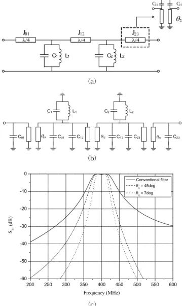
Firstly, the generalized bandpass filter model provided by
Matthaei (1980)is employed to design the target filter, as
shown in Fig. 7. A bandpass filter with two resonators
based on this model is offered in Fig. 8 (a), with the help
of the following equations (12)~(16):
'
A 1 01
0 1 1
Y l w J = g g w
(12)
j j+1 j, j+1 j=1 to n-1
1 ' j j+1
w l l J |
w g g
=
(13)
B n n,n+1
n n+1 1 '
Y l w J = g g w
(14)
( )
j 0 j
0 j
l C 1 j 1, 2, ,n
ω L
= = ω = ....
(15)
1 ' 1
w = (16)
where , and = inverter parameters;
= susceptance slope parameters;
= element values in Chebyshev low-pass prototype;
, = lumped capacitors and inductors.
Then the admittance inverter, which is quarter-wave transmission line with normalized characteristic admittance
can be miniaturized using the method introduced in last section, as shown in Fig. 8 (a), (b), where is the electrical length of each stage in the miniaturized filter and
is the corresponding capacitors. As two examples, here we reduced the electrical length to 45 and 7 degrees, respectively. However, Fig. 8 (c) shows that the size-reduced bandpass filters have narrower bandwidth than that of the conventional one. According to Fig. 8 (c), the bandwidth of conventional bandpass filter with -1dB insertion loss is 45MHz. The miniaturized one with
° is 38MHz and ° is 29MHz. Due to this bandwidth shrinkage the miniaturized filter deviated from the target.
In addition, the adoption of generalized bandpass filter design method results in different values of inverter characteristic admittance . Thus, the capacitors
also have different values. This is not convenient since the commercialized lumped capacitors can not support the various capacitor values. And because some other artificial resonators were inserted in the procedure of miniaturization, the designed susceptance slope parameters already changed. Therefore the original resonators became unnecessary. For these reasons, we will not adopt the generalized bandpass filter model for designing extremely miniaturized bandpass filter.
Instead, the circuit in Fig. 9 is considered to be the model that can be miniaturized using the size-reduction method introduced in section 3. More stages can be achieved simply by connecting several of the same circuits.
To prove this discussion, ADS is used to simulate 1-, 2- and 3-stage proposed compact bandpass filters. It is worth noting that the stage number mentioned in this paper is not determined by the resonators as usual, but rather it is the
Y
AJ 01 C
1L
1J 12 C
2L
2…… C
nL
nJ
n,n+1Y
BFig. 7 A generalized bandpass filter circuit using admittance inverters.
(a)
(b)
200 250 300 350 400 450 500 550 600
-60 -50 -40 -30 -20 -10 0
Conventional filter θ
ij= 45deg θ
ij= 7deg
S 21 (dB )
Frequency (MHz)
(c)
Fig. 8 Designed filter based on the generalized bandpass
filter. (a) Conventional filter, (b) miniaturized filter,
(c) simulated results.
Fig. 9 Model of one-stage bandpass filter used in this paper.
(a)
200 240 280 320 360 400 440 480 520 560 600
-40 -30 -20 -10 0
S
21(d B )
Frequency (MHz) 1 stage
2 stages 3 stages
(b)
0 1 2 3 4 5
-260 -240 -220 -200 -180 -160 -140 -120 -100 -80 -60 -40 -20 0
3 stages 2 stages
S
21(d B )
Frequency (GHz) 1 stage
(c)
Fig. 10 (a) ADS model of the miniaturized 1-stage 7-degree filter, (b) simulated results of 1-, 2- and 3-stage 7-degree filters for comparison of slope characteristics, (c) broadband characteristics.
inverter number. In other words, an n-stage miniaturized filter means it consists of n pairs of coupled line, and the inverter number of original filter is n. Since the port characteristic impedance is 50Ω, the inverter characteristic impedance should also be 50Ω. The electrical length of the coupled line in miniaturized filter was chosen to be 7 degrees, and by fixing as 70Ω, we can get the value
of as 52.2Ω using equation (11). The capacitor value was obtained with (10), and is given in Fig. 10 (a). The skirt characteristic improves as more stages are connected in series, shown in Fig. 10 (b), but in fabrication the use of many stages will inevitably result in a large insertion loss.
The broadband characteristics in Fig. 10 (c) show good suppression of spurious passbands. This is because the lumped capacitors are used as resonators while the conventional bandpass filter has the structure that half-wave transmission lines are used as resonators.
Therefore, these lumped capacitors suppress the harmonics resulting from distributed circuits effectively.
Bandwidth is an important parameter of bandpass filter.
The bandwidth of the proposed filter is closely related to
the coupling coefficient
of the short-ended
coupled line(Kang, 2003). The larger the coupling coefficient K, the broader the bandwidth of the filter, as illustrated in Fig. 11, where the electrical length of the coupled line is chosen as 7º and two stages are used. When we miniaturize the quarter-wave transmission line, we can choose a proper coupling coefficient according to the bandwidth of the required bandpass filter. However, to achieve a broad bandwidth, the coupling coefficient K should be made as large as possible, which means the difference between and should be large. It will result in a small ′ and hence a large electrical length of the coupled line. Therefore, a trade-off is needed between broad bandwidth and small circuit size.
200 240 280 320 360 400 440 480 520 560 600
-40 -30 -20 -10 0
K 3 K 2 S 21 (d B)
Frequency (MHz)
K 1 = 0.11 K 2 = 0.14 K 3 = 0.17 EL=7 deg
K 1
Fig. 11 Relation between the bandwidth and coupling
coefficient of the coupled line (electrical length of
the coupled line is chosen as 7 º and two stages
are used).
The proposed bandpass filter can be categorized as combline filters. However, it has the following new features:
Firstly, compared with conventional combline filters, an inter-stage transmission line has been used to prevent the unwanted coupling between the two neighboring resonators.
And distortions will appear if this inter-stage transmission line is too short or not used. The further discussion is in the next section.
Secondly, there are resonance circuits at both the input and output ports. In a traditional combline filter, the short-ended transmission lines used as input and output are equivalent to shunt inductors, as illustrated in Fig. 12 (Matthaei, 1980). If is small, inductance L is tremendously small and nearly short. Therefore, the signals can not flow into the filter, which hindered the miniaturization of the traditional combline filters. Actually, the electrical length of the traditional combline filter was generally recommended as 45º or less in(Matthaei, 1980).
On the contrary, in this new design theory #0 and #n+1 resonators naturally appear because artificial resonators were added for the purpose of miniaturizing quarter-wave transmission line.
Fig. 12 Equivalent circuit of the iutput and ouput sections in the conventional combline filters.
Thirdly, the size of the parallel coupled line in the modified combline filter can be extremely miniaturized
according to ′
, so long as we choose ≈ .
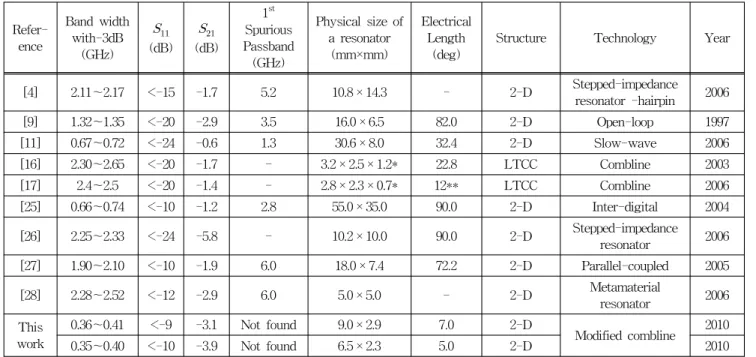
No combline filter as small as a few degrees has been published, to the authors’ knowledge.
A compact bandpass filter is found in (Kang, 2007), which is miniaturized based on Hitota’s theory. The modified combline bandpass filter discussed in this paper is built on the lumped model of a quarter-wave transmission line.
5. Simulation and Fabrication
To confirm the above theory, two bandpass filters working at 400MHz were designed and fabricated on a Taconic Teflon substrate with relative permittivity =3.56, thickness=0.762mm and the copper thickness=34um. Firstly, a filter with the electrical length of the coupled line being 7º, named 7-degree filter, was designed. The value of the lumped capacitors was calculated to be 54.2pF. The odd impedance of the coupled line was 52.2Ω when the even mode impedance was fixed at 70Ω, making the coupling coefficient being 0.14. The length of the coupled line was calculated to be 9mm, while the width of each line was 1.1mm and the slot of the coupled line was 0.7mm.
Before fabrication, simulation using HFSS was done for a proper center frequency and a good insertion loss, which will be detailed in the following few graphs.
According to the simulation, the use of theoretical 54.2pF MIM capacitors has shifted center frequency to 350MHz due to the length of via hole. So here, 45pF capacitors were used to move it back to the predicted 400MHz. As a rule of thumb, the midband of the proposed modified bandpass filter increases as the capacitor value decreases, and vice versa.
As mentioned in last section, the utilization of inter-stage transmission line between two neighboring stages is a new feature compared with the conventional combline bandpass filter. In this type of conventional filter, coupling between resonators is achieved by way of the fringing fields between resonator lines each other. However, the parallel short-ended coupled line with loading capacitors in the proposed filter is the equivalent of the inverter and the inverters were connected in original filter. Therefore, the neighboring line pair should be connected using inter-stage transmission line to limit the coupling within each pair of coupled line. If this inter-stage line is not included, shown in Fig. 13 (a), distortion appears. To show its importance more clearly, particular simulations in HFSS have been done. Fig. 13 (b), which gives the simulated results according to different distance between two stages, indicates that the performances are unsatisfactory. The distortion can be eliminated by using inter-stage transmission line, as illustrated in Fig. 14 (a). At first a 50 Ω transmission line with the length ′ of 0.7mm is added between two stages. However, distortion still occurs, as can be seen from the performance given in Fig. 14 (b).
When the length is increased to 3mm, distortion gets less
severe and improves. Here, a length of 5mm connection transmission line is adopted in fabrication for a good insertion loss and proper center frequency.
(a)
200 250 300 350 400 450 500 550 600
-60 -50 -40 -30 -20 -10 0
S
21(dB )
Frequency (MHz)
L
i= 0.7 mm L
i= 3.0 mm L
i= 5.0 mm
(b)
Fig. 13 Simulated results of 7-degree filter according to different inter-stage distance. (a) Circuit, (b) insertion loss.
(a)
200 250 300 350 400 450 500 550 600
-30 -25 -20 -15 -10 -5 0
S
21(dB)
Frequency (MHz)
L
i'= 0.7 mm L
i'= 3.0 mm L
i'= 5.0 mm
(b)
Fig. 14 The insertion loss performances of 7-degree filter according to different inter-stage connecting transmission line. (a) Circuit, (b) insertion loss.
It is insisted by some authors that the performances can be improved by tapping the input and output resonators(
Kuo, 2003). However, in this proposed filter, connecting of different stages must be done at the fixed points for matching. As illustrated in Fig. 15 (a), connection points must be at A and B. If A’ (A”) and B’ (B”) are used for connection, mismatching will occur between two neighboring stages. This point can be better supported by the simulation of the above 7-degree filter given in Fig. 15 (b), where mm.
(a)
100 200 300 400 500 600 700 800
-70 -60 -50 -40 -30 -20 -10 0
S
21(d B )
Frequency (MHz)
AB A'B' A"B"
(b)
Fig. 15 (a) Position for connecting the input and output of independent bandpass filters, (b) simulated
performances of 7-degree filter according to different connection points.
Fig. 16 The photo of the designed two-stage 7-degree
bandpass filter with a midband of 400 MHz.
The size of the fabricated 7-degree filter is available in Fig.
16, with one resonator taking up a circuit area of 9×2.9mm².
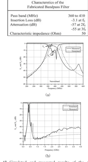
Fig. 17 gives the simulated results of the fabricated filter using Ansoft HFSS and the measured ones with Agilent 8722ES Network Analyzer. Some detailed performances are offered in Table 1. The measured center frequency is shifted from 400MHz to the left by 15MHz due to two reasons. The first one is the difference between MIM capacitors and lumped capacitors. In HFSS, MIM capacitors should be used to carry out simulation. However, in fabrication only lumped capacitors were available. The MIM capacitor value calculated through is actually a little larger than that needed, due to the fringing effect. The other reason is that the lumped capacitors have an ± error that can’t be predicted.
The spurious passband of the proposed passband filter does not appear or is very away from the passband, as a result of the small length of the coupled line, as shown in Fig. 17 (b).
In fact, the first spurious was not observed even up to 11GHz during measurement.
Table 1 Measured performances of 400 MHz 7-degree filter
200 250 300 350 400 450 500 550 600
-60 -50 -40 -30 -20 -10 0
S
11and S
21(dB )
Frequency (MHz)
Measured Simulated
Narrowband S
21S
11(a)
0.0 0.5 1.0 1.5 2.0 2.5 3.0 3.5 4.0
-70 -60 -50 -40 -30 -20 -10 0
S
11an d S
21(dB )
Frequency (GHz)
Simulated Measured
(b)
Fig. 17 Simulated and measured results of the designed two-stage 7-degree bandpass filter. (a) Narrowband response, (b) broadband response.
It is flexible to choose the electrical length of the coupled line. For a specified bandwidth, it is up to the designer. To prove that, another bandpass filter, with the electrical length of the coupled line being 5º has been designed. To get a similar bandwidth, the coupling coefficient K of the coupled line is made approximately to be 0.14 by choosing
90Ω and 68.5Ω, respectively. The length of the coupled line is calculated to be 6.5mm, areduction of 28%
with respect to the7-degree filter. Fig. 18 gives the simulated and measured results of the 5-degree filter, compared with the performances of 7-degree filter. The center frequency of the 5-degree filter is also shifted as a result of the inexact capacitor value.
200 250 300 350 400 450 500 550 600
-60 -50 -40 -30 -20 -10 0
5 degree
Simulated Measured
S
21(d B)
Frequency (MHz) 7 degree
(a)
200 250 300 350 400 450 500 550 600
-30 -25 -20 -15 -10 -5 0