접수일자 : 2014. 05. 09 심사완료일자 : 2014. 05. 29 게재확정일자 : 2014. 06. 13
* Corresponding Author Dong-You Choi(E-mail:[email protected], Tel:+82-62-230-7060)
Department of Information and Communication Engineering, Chosun University, 309 Pilmun-daero Dong-gu, Gwangju 501-759, Republic of Korea
Open Access http://dx.doi.org/10.6109/jkiice.2014.18.8.1785 print ISSN: 2234-4772 online ISSN: 2288-4165 This is an Open Access article distributed under the terms of the Creative Commons Attribution Non-Commercial License(http://creativecommons.org/li-censes/
한국정보통신학회논문지(J. Korea Inst. Inf. Commun. Eng.) Vol. 18, No. 8 : 1785~1790 Aug. 2014
2.45 ㎓에서 무선 통신 시스템을 위한 인셋 페드 마이크로스트립 패치 안테나
사지나 프라다한1 · 최동유2*
Inset Fed Microstrip Patch Antenna for Wireless Communication at 2.45 ㎓
Sajina Pradhan1 · Dong-you Choi2*
1Department of Electronic Engineering, Chosun University, 309 Pilmun-daero Dong-gu, Gwangju 501-759, Republic of Korea
2*Department of Information and Communication Engineering, Chosun University, 309 Pilmun-daero Dong-gu, Gwangju 501-759, Republic of Korea
요 약
통신 시스템에서 다양한 종류의 마이크로스트립 안테나는 많은 어플리케이션에서 사용되고 있다. 본 논문에서는
무선통신을 위한 2.45 ㎓의 인셋 페드 직사각형 마이크로스트립 패치 안테나를 HFSS를 활용하여 설계하였다. 안테
나는 유전율 2.2, 두께 1.6 ㎜의 Telfron 기판을 사용하였으며 기판의 한쪽 면은 접지면을 갖는다. 시뮬레이션을 통하 여 반사손실, VSWR, 이득, 방사패턴 등의 안테나 특성을 확인하였다.
ABSTRACT
In communication systems, there are various types of microstrip antenna that can be used for many applications.
This paper mainly focuses on the simple design of inset fed rectangular microstrip patch antenna to operate at frequency of 2.45 GHz for wireless communication. The study involves using HFSS simulator to design the antenna dimensions and to determine its performance. This antenna is based on a thickness of 1.6㎜ Teflon substrate with a dielectric constant of approximately 2.2, on one side of the substrate and another side has a ground plane. After simulation, the antenna performance characteristics such as return loss, VSWR, gain, radiation pattern are obtained.
키워드 : 마이크로스트립 패치 안테나, 인셋 페드 기술, 무선 통신
Key word : Microstrip Patch Antenna, Inset Fed Technique, Wireless Communication
Ⅰ. Introduction
Wireless communication has a great impact on human life since it has been developed rapidly in the past decades. In the field of wireless communications, antenna plays a vital important role. During late 1970s, there was rapid development in the field of microstrip patch antenna technology. During early 1980s, antenna elements and arrays were developed in term of design and modeling. The antenna have been largely studied due to their advantages like light weight, reduced size, low cost, conformability and the ease of integration with active device. A microstrip patch antenna is the combination of a radiating patch on one side of the dielectric substrate and ground on the other side. The patch is generally made of conducting material like gold or copper. On the dielectric substrate, the radiation patch and the feed lines are usually photo etched. Microstrip patch antennas radiate primarily because of the fringing fields between the patch edge and the ground plane.
Therefore, the antenna can be fed by the various methods. These methods can be classified into two categories one is contacting and another is non-contacting. In the contacting method, the radio frequency power is directly fed to the radiating patch by using a connecting element such as microstrip line or probe feed. Whereas, in case of the non-contracting method, electromagnetic field coupling is done to transfer power between the microstrip line and the radiating patch which includes proximity feeding and aperture feeding [1, 2].
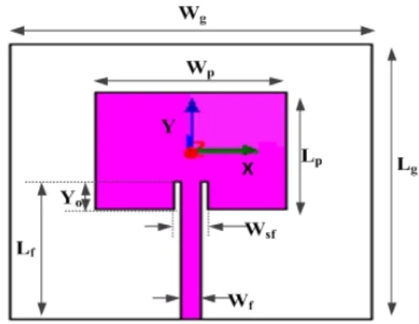
Microstrip patch antenna is characterized by a large number of physical parameters. They are designed to have many geometrical shapes and dimensions but rectangular and circular microstrip patches have been used in many applications. In this paper, the design of inset fed rectangular microstrip patch antenna at 2.45 ㎓ for wireless communication is presented having length of the patch Lp, width of the patch Wp, length of ground plane Lg, width of the ground plane Wg, inset fed distance Yo, transmission line length Lf and width Wf
and Wsf is the width of the gap as shown in Figure 1.
This antenna is designed on Teflon and its performance characteristic such as Return loss, VSWR, gain, radiation pattern are obtained from the simulation.
그림 1. 인셋 페드 사각형 마이크로스트립 패치 안테나 Fig. 1 Inset Fed Rectangular Microstrip Patch Antenna
Ⅱ. Antenna Geometry and Its Design Requirement
For a rectangular patch, the length L of the patch is usually 0.3333λ0 is the free sapace wavelength. The patch is selected to be very thin such that the height of substrate h≪λ0. Thus, a rectangular patch of dimension 38.6 ㎜ × 48 ㎜ is designed on oce side of Teflon substrate of thickness 1.6 ㎜ and the ground plane of 90
㎜ × 90 ㎜ are located on the other side of the substrate.
There are three essential parameters for design of inset fed rectangular microstrip patch antenna. They are resonant frequency (fr), dielectric material of the substrate (εr) and the thickness of substrate. The resonant frequency chosen for this design is 2.45 ㎓.
The dielectric material of the substrate chosen for this antenna design is Teflon having a dielectric constant of the 2.2 and the loss tangent equal to 0.0009. For design purpose, the dielectric constant of the substrate material is also an important parametric factor. Low dielectric constant of the substrate material is used in the design
because it gives better efficiency, higher bandwidth and the low quality factor Q. The low value of dielectric constant increases the radiated power. The designed has patch size independent of dielectric constant. So, the reduction of patch size is by using higher dielectric constant and Teflon is good in this agreement. In the simulation, the small loss tangent was neglected.
Thickness of substrate is another important in design parameter. Since thick value of substrate increases the fringing field of the patch periphery like low dielectric constant and also increases the radiated power. The dielectric substrate height of the inset fed microstrip patch antenna is h = 1.6 ㎜.
Ⅲ. Mathematical Calulation of The Antenna Parameters
The parameters of the antenna can be calculated by the transmission line method [1, 3].
3.1. Width of the Patch
The width of the antenna can be determined by
(1)Where,
c = velocity of light fr = resonance frequency
εr = dielectric constant of substrate WP = Width of the patch
3.2. Length of the patch
The effective dielectric constant can be determined by
(2)Where, εreff = effective dielectric constant
εr = dielectric material of substrate h = height of dielectric substrate Wp = width of the patch
The dimensions of the patch along its length have been extended on each end by distance, the extension length is given by
(3)
The actual length L of the patch is given by
(4)
Where, fr is the resonance frequency[4]
3.3. Inset fed of the patch antenna
A physical notch is introduced by the inset feed, which in turn introduces a junction capacitance. The physical notch and its corresponding junction capacitance influence the resonance frequency. As the inset feed-point moves from the edge toward the centre of the patch the resonant input impedance decreases monotonically and reaches zero at the centre. When the value of the inset feed point approaches the centre of the patch, the
where is inset distance, which
varies very rapidly; therefore the input resistance also changes rapidly with the position of the feed point. For maintaining very accurate values, a close tolerance has to be preserved [5-10]. In this paper, the value of inset fed distance is 9.3 ㎜ and the length and width of transmission line at 50 Ω is 45 ㎜ and 5 ㎜ respectively.
The following Table 1 gives the detail design parameter specification of microstrip patch antenna[11].
Ⅳ. Simulation Result
The antenna was simulated in HFSS (High Frequency Structure Simulation) which is a high performance full-wave electromagnetic (EM) field simulator for arbitrary 3D volumetric passive device, having Microsoft windows graphical user interface. The designed antenna in HFSS simulator is shown in Figure 2.
표 1. 마이크로스트립 패치 안테나의 설계 파라미터 Table. 1 Design parameter of microstrip patch antenna
Type of the antenna Rectangular Patch Antenna Dielectric constant of the
substrate (εr) 2.2
Dielectric substrate material
used Teflon
Height of the dielectric
substrate (h) 1.6 mm
Operating frequency (fr) 2.45 GHz Feeding method Microstrip inset line
feed
Polarization Linear
Dielectric loss tangent (tanδ) 0.0009 Length of the patch (Lp) 38.6 mm Width of the patch (WP) 48 mm Length of the feed line (Lf) 45 mm Width of the feed line (Wf) 5 mm Length of the ground plane (Lg) 90 mm Width of the ground plane (Wg) 90 mm Width of the gap (Wsf) 8.5mm Inset feed distance (Yo) 9.3 mm Impedance Matching (Zo) 50 Ω
그림 2. HFSS로 설계된 안테나 Fig. 2 Design Antenna in HFSS
The simulation result of return loss of the inset fed antenna is -33.66 ㏈ at center frequency of 2.45 ㎓ as shown in Figure 3.
그림 3. 반사손실 vs. 주파수 Fig. 3 Return Loss vs. Frequency
he bandwidth of the antenna in term of percentage is defined by
m ax m in
× (5)
Where, fmax and fmin are determined at -10 ㏈. fr is the resonance frequency. The simulated value at -10 ㏈, fmax
= 2.48 ㎓, fmin = 2.42 ㎓, BW = 60 ㎒ and the bandwidth percentage is 2.44%.
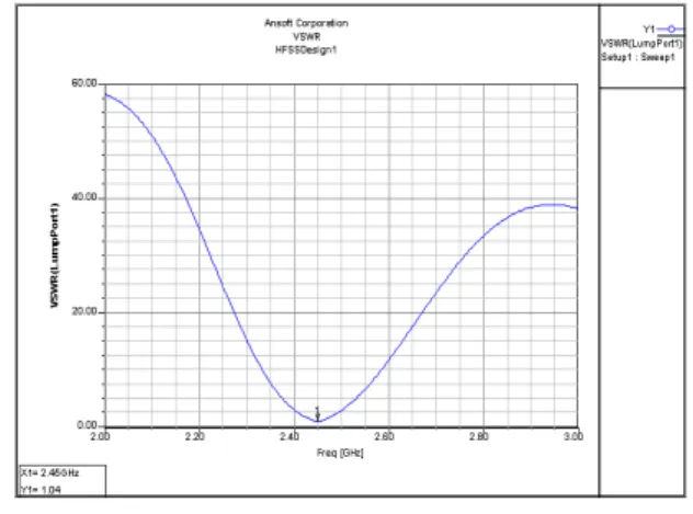
그림 4. VSWR vs. 주파수 Fig. 4 VSWR vs. Frequency
The VSWR characteristic of the antenna should falls in between 1 to 2. From simulation its value is 1.04 at 2.45 ㎓ as depicted in Figure 4.
Also the radiation pattern of the antenna obtained is shown in Figure 5 at phi = 90°and phi = 0° at 2.45 ㎓.
The 3D polar plot of gain is shown in Figure 6 which shows the gain of 6.9 ㏈.
그림 5. 2.45 ㎓ 방사 패턴
Fig. 5 Radiation Pattern at 2.45 ㎓
그림 6. 전체 이득의 3D Polar Plot Fig. 6 3D Polar Plot of total gain
The scattering parameter for the antenna design at 2.45 ㎓ on the smith chart is shown in Figure 7.
그림 7. 2.45 ㎓ 스미스 차트 Fig. 7 Smith chart at 2.45 ㎓
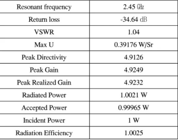
Table 2 summarizes the obtained simulation features of the antenna from high frequency simulation software.
표 2. 마이크로스트립 패치 안테나의 시뮬레이션 결과 Table. 2 Simulation results of microstrip patch antenna
Resonant frequency 2.45 ㎓
Return loss -34.64 ㏈
VSWR 1.04
Max U 0.39176 W/Sr
Peak Directivity 4.9126
Peak Gain 4.9249
Peak Realized Gain 4.9232
Radiated Power 1.0021 W
Accepted Power 0.99965 W
Incident Power 1 W
Radiation Efficiency 1.0025
Ⅴ. Conclusion
In this paper, the mathematical calculation for design of inset rectangular patch antenna at 2.45 ㎓ is presented. Simulation of inset fed microstrip patch antenna is done in HFSS. The antenna performance characteristics such as return loss, VSWR, gain, radiation pattern are obtained in simulation. Hence, from simulation, the return loss obtained is -34.64 ㏈ at
2.45 ㎓; VSWR is 1.04 and gain about 6 ㏈. In future, the simulated antenna can be fabricated in PCB Board.
Acknowledgement
This study was supported by research fund from Chosun University, 2014
REFERENCES
[ 1 ] Constantine A. Balanis "Antenna theory analysis and design" 2nd edition.
[ 2 ] David M. Pozar "Microwave Engineering" 2nd edition.
[ 3 ] www.eurojournals.com/ejrs.htm
[ 4 ] Sika Shrestha, Sun-Kuk Noh and Dong-You Choi,
"Comparative Study of Antenna Designs for RF Energy Harvesting," International Journal of Antennas and Propagation," Vol. 2013, pp. 1-10, 2013.
[ 5 ] Ying Hu, David R. Jackson, Jeffery T. Williams, and Stuart A. Long, "A Design Approach for Inset-Fed Rectangular Microstrip Antennas," IEEE, Antennas and Propagation
Society International Symposium 2006, pp. 1491-1494, Jul.
2006.
[ 6 ] M. Ramesh, YIP KB, "Design Formula for Inset Fed Microstrip Patch Antenna," Journal of Microwave and Optoelectronics, Vol. 3, No. 3, Dec. 2003.
[ 7 ] Indra Surjati, Yuli KN and Arky Astasari "Microstrip Patch Antenna Fed by Inset Microstrip Line For Radio Frequency Identification (RFID)," Electromagnetic Compatibility, pp.
1351-1353, Apr. 2010.
[ 8 ] M A Matin, A. I. Sayeed, “A Design Rule for Inset-fed Rectangular Microstrip Patch Antenna,” WSEAS TRANSACTIONS on COMMUNICATIONS, Vol. 9, pp.
63-72, Jan. 2010.
[ 9 ] Lorena I. Basilio, Michael A. Khayat, Jeffery T. Williams, Stuart A. Long, “The Dependence of the Input Impedance on Feed Position of Probe and Microstrip Line-Fed Patch Antenna,” IEEE TRANSACTIONS ON ANTENNAS AND PROPAGATION, Vol. 49, No. 1, pp. 45-47, Jan. 2001.
[10] Ayesha Aslam, F A Bhatti, “Improved Design of Linear Microstrip Patch Antenna Array,” 2010 9th International Symposium, Antennas Propagation and EM Theory, pp.
302-306, Dec. 2010.
[11] Dong-You Choi, Sika Shrestha, Jung-Jin Park and Sun-Kuk Noh, "Design and Performance of an Efficient Rectenna Incorporating a Fractal Structure," International Journal of Communication System, DOI: 10.1002/dac.2587, Jul. 2013.
Sajina Pradhan
received M.S. degree in the Department of Information and Communication Engineering from Chosun University, Gwangju, Korea in 2012. Since 2012, she has been an Ph.D. student in the Department of Electronic Engineering from Chosun University, Gwangju, Korea. The research areas of interest are Signal processing, RF energy harvesting devices, designs and applications.
Dong You Choi
Dong You Choi was born in Seoul, Korea, on February 25, 1971. He received the B.S., M.S. and Ph.D. degree in the Department of Electronic Engineering from Chosun University, Gwangju, Korea in 1999, 2001, and 2004, respectively. Since 2007, he has been taught and researched as a professor at Chosun University. His research interests include mobile communication and wave propagation. He is a member of IEEE, IEICE, JCN, KEES, IEEK, KICS, and ASK.