반사판을 갖는 인셋 급전 CSLR 패치 안테나 제작
홍재표*ㆍ김병문**ㆍ손혁우***
Fabrication of CSLR-loaded Inset Fed Patch Antenna with a Conducting Reflector
Jae-Pyo Hong
*ㆍByung-Mun Kim
**ㆍHyeok-Woo Son
***요 약
본 논문에서는 인셋 급전한 패치의 접지면에 Complementary Single Loop Resonators(: CSLRs)을 배열한 안테나의 복사패턴을 개선하기 위하여 도체 반사판 사용을 제안하였다. 제안된 안테나의 반사판은 패치의 접 지면으로부터 약
아래에 위치하고, 크기는 패치의 약 2배 정도이다. 유전율 2.5, 두께 0.787 mm인 마이 크로스트립 기판을 사용하여 안테나를 설계, 제작하여 실험하였고, Finite Element Method(: FEM) 기반의 3D EM Solver인 HFSS를 사용하여 시뮬레이션 하였다. 실험결과, 반사판이 있는 경우의 안테나 공진주파수와 정 합특성은 반사판이 없을 때와 거의 동일하게 변화가 없었으나, 복사패턴은 반사판에 의해 상당히 개선되었음 을 확인하였다.
ABSTRACT
In this paper, we propose the CSLR(: Complementary Single Loop Resonators)-loaded inset fed patch antenna with a conducting reflector to improve the radiation patterns. Reflector of the proposed antenna is located below about
from the ground plane of the patch, the size is about two times of the patch. The proposed antenna is designed and fabricated on the substrate which has a dielectric constant and thickness with 2.5 and 0.787 mm, respectively. Simulation results are obtained by using the HFSS, 3D EM Solver based Finite Element Method(: FEM). The resonant frequency and matching characteristics of the antenna with reflector are substantially the same as when there is no change in the antenna without reflector, it is confirmed that radiation patterns are significantly improved by the reflector키워드
Inset Fed Microstrip, Patch Antenna, CSLR, Reflector 인셋 급전 마이크로스트립, 패치 안테나, CSLR, 반사판
* 주저자 : 경일대학교 전자공학과([email protected])
** 경북도립대학교 IT특약계열([email protected])
*** 교신저자 : ㈜한화 ㆍ접 수 일 : 2016. 10. 03 ㆍ수정완료일 : 2016. 11. 13 ㆍ게재확정일 : 2016. 11. 24
ㆍReceived : Oct. 03, 2016, Revised : Nov. 13, 2016, Accepted : Nov. 24, 2016 ㆍCorresponding Author : Hyeok-Woo Son
Hanwha Corporation Email : [email protected]
Ⅰ. 서 론
메타물질은 자연에 존재하지 않는 인위적인 물질이 며, 유전율과 투자율이 음인 물질이다. 이러한 메타물
질을 특성을 실제 구현할 수 있는 대표적인 구조는
SRR(: Split Ring Resonator)과 SLR(: Single Loop
Resonator)이다. SRR은 2개의 분리된 도선 링 공진기
가 서로 반대방향의 갭을 갖는 구조이고, SLR은 하나
http://dx.doi.org/10.13067/JKIECS.2016.11.11.1047
의 링으로 된 공진기인 구조이며, 현재 많은 연구가 진행되고 있다[1-5]. 또한 이를 접지면의 도선부분을 식각한 CSRR과 CSLR 구조에 대한 연구도 진행되고 있으며, 안테나의 소형화 연구에 응용되고 있다[6-12].
그리고 반사판을 이용하여 안테나의 이득과 지향성을 개선한 연구가 있다[5].
본 논문에서는 반사판을 이용하여 패치의 접지면에 CSLR을 배열한 안테나의 복사패턴을 개선하였다. 안 테나의 소형화를 구현하기 위해 패치의 접지면에 SLR을 식각한 CSLR을 배열하여 패치의 크기를 소형 화 하였으나, CSLR이 있는 접지면으로의 후방 복사 가 발생하여 접지면으로부터
떨어진 위치에 도 체 반사판을 배치한 안테나를 제안하였다. 여기서 λ0 는 자유공간 파장이다. 그리고 유전율 2.5, 두께 0.787 mm인 마이크로스트립 기판을 사용하여 안테나의 반 사손실과 복사패턴을 계산한 후 안테나의 특성을 비 교 분석하였다. FEM 기반의 3D EM Solver인 HFSS 를 사용하여 시뮬레이션을 수행하였다.
Ⅱ. 제안한 안테나 구조와 설계
2.1 반사판을 갖는 인셋 급전 CSLR 안테나 구조
그림 1. 반사판을 갖는 인셋 급전 안테나 구조 Fig. 1 Geometry of inset fed microstrip antenna
with reflector
그림 1은 본 논문에서 제안한 안테나 구조로서 인 셋 급전된 마이크로스트립 패치 안테나의 접지면에 CSLR을 배열하였고, 접지면 아래에는 반사판을 배치 하였다. 패치의 폭과 길이는 각각 Patch_W, Patch_L, 인셋의 폭과 길이는 Inset_W, Inset_L, 급전선의 폭과 길이는 Inset_W, Inset_L이다. 마이크로스트립 유전체 의 유전율과 두께는 각각 ε
r, Sub_h이다. 그리고 가운 데 면은 패치 안테나의 접지면이며, 안테나의 소형화 를 위해 접지면에 CSRR과 유사한 구조인 CSLR을 적절하게 배열하여 안테나를 소형화하였다. 그리고 안 테나의 복사패턴을 개선하기 위하여 CSLR을 갖는 접 지면 아래 Air_h 위치에 반사판을 위치하도록 제안하 였다. 그리고 반사판의 길이와 폭은 각각 Reflector_L, Reflector_W이다. 시뮬레이션을 통해 최적화된 안테 나의 파라미터 값들은 표 1에 제시된 바와 같다.
표 1. 제안된 안테나 파라미터 Table 1. Designed antenna parameters
Parameter Value
Patch
Patch length 22.90 mm
Patch width 25.20 mm
Inset fed length 6.16 mm Inset fed width 2.80 mm
Ground
Array of CSLRs 3×3
Ground length 45.30 mm
Ground width 50.40 mm
Reflector
Distance between ground and
reflector 7.0 mm
Ground length 80.00 mm
Ground width 90.00 mm
2.2 SLR 단위 셀 구조
그림 2. 단일 SLR 구조
Fig. 2 Geometry of unit SLR
그림 2는 단일 SLR 정사각형 구조이며, 바깥쪽 도 선의 최대 길이는 SLR_L, 도선의 폭은 S_W, 인접한 도선사이의 분리된 간격은 s, 공진기를 형성하는 도선 사이의 간격은 gap이다. 그리고 단일 SLR을 형성하 는 전체 유전체의 길이는 Cell_L이다[2-5]. 그리고 CSLR의 단일 구조의 제원은 참고문헌[3-5]의 결과와 동일하며, 패치 아래 접지면에 3×3 배열로 배치하였 다.
Ⅲ. 제안한 안테나 제작 및 측정
3.1 안테나 제작 및 실험
제작된 안테나는 그림 3과 같다. 그림 3(a)은 안테 나의 윗면이며, 패치 안테나는 인셋 구조로 급전되었 고 유전율 2.5, 두께 0.787 mm인 기판을 사용하여 제 작하였다. 그리고 접지면의 아랫부분에 반사판이 위치 하였다. 적용된 반사판은 단면 기판의 도체 면을 사용 하였으며, 위치 고정은 공기와 거의 같은 유전율을 갖 는 7mm 두께의 스티로폼(Styrofoam, 유전율 1.03)을 사용하였다. 그림 3(b)는 접지면에 3×3으로 배열 배치 된 CSLR을 보여주고 있다.
(a)
(b)
그림 3. 제작된 안테나 (a) 윗면 (b) 접지면 Fig. 3 Proposed antenna (a) top (b) ground
안 테나의 복사패턴은 경북대학교에 있는 전파 무반사 실에서 측정하였다. 그림 4(a)에서와 같이 제작된 안테 나를 송신 안테나로 사용하여 360도 자동으로 복사 패 턴을 측정하였다. 그리고 그림 4(b)와 같이 표준 안테나 인 혼안테나를 수신 안테나로 실험하여 측정하였다.
(a)
(b)
그림 4. 복사패턴 측정 (a) 제작된 안테나 (b) 무반사실
Fi.g. 4 Photograph of measurement for radiation pattern with (a) the fabricated antenna in (b) anechoic
chamber
3.2 안테나 측정결과
그림 5는 반사판이 있는 안테나에 대한 반사손실을
측정한 결과를 나타낸 그림이다. 그림에서와 같이 측
정된 안테나의 공진주파수는 2.90 GHz이고, 반사손실
은 약 -19.90 [dB]이다. 이는 동일한 안테나에 대해
반사판이 없는 참고문헌[3-5]의 이론적인 결과인 공
진주파수 2.82 GHz에서 반사손실은 -29.82와 거의 동
일함을 알 수 있다. 그림 6은 본 논문에서와 같이 반
사판이 없는 동일한 안테나[3-5]에서의 연구 결과를
나타내며, 2.885 GHz에서의 E-면과 H-면 복사패턴에
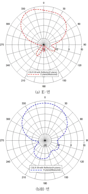
대한 실험 결과이다. 그림 7은 본 논문에서 제안한 방
법인 접지면으로부터
떨어진 위치에 반사판을
설치한 안테나의 복사패턴을 측정한 결과이며, 그림
7(a)와 7(b)는 2.885 GHz에서 각각 E-면과 H-면 복
사패턴에 대한 결과를 나타낸다.
그림 5. 안테나의 측정된 반사손실 Fig. 5 Measured radiation loss of the antenna
그림 6. 반사판이 없는 CSLR 인셋 급전의 측정 복사패턴
Fig. 6 Measured radiation pattern of the antenna without a reflector
(a) E-면
(b)H-면
그림 7. 반사판이 있는 CSLR 인셋 급전의 측정 복사패턴 (a) E-면 (b) H-면
Fig. 7 Measured radiation pattern of the antenna with a reflector (a) E-plane (b) H-plane
본 논문에서 제안한 바와 같이 반사판을 갖는 안테
나의 복사패턴인 그림 7의 결과는 반사판이 없는 안
테나의 결과인 그림 6과 비교하면 후방으로의 복사패
턴이 개선됨을 확인할 수 있다.
Ⅳ. 결 론
본 논문에서는 안테나의 접지면에 CSLR을 배열하 여 안테나의 소형화와 접지면으로부터
떨어진 위치에 반사판을 위치하여 복사패턴을 개선하기 위한 안테나를 제작 실험하여 안테나의 복사패턴을 측정하 여 기존 결과와 비교하였다. 그 결과 반사판을 인가함 으로써 안테나 후방으로부터의 복사가 감소된 양호한 결과를 실험적으로 확인하였다.
감사의 글
본 논문은 2016년도 한국전자통신학회 춘계 종 합학술대회 우수논문을 확장한 논문임.
References
[1] M. Yoo and S. Jim, “SRR- and CSRR-loaded ultra-wideband (UWB) antenna with tri-band notch capability,” J. of Electromagnetic Waves and Applications, vol. 27, no. 17, 2013, pp.
2190-2197.
[2] J. Hong and B. Mim, "Design of inset fed patch antenna loaded with complementary single loop resonator," Proc. of the Korea Institute of Electronic Communication Sci- ences 2014 Conf., Pusan, Korea, vol. 8, no. 1, June, 2014, pp. 127-130.
[3] J. Hong and B. Mim, “A study on inset fed microstrip antenna loaded with complementary single loop resonator," J. of the Korea Institute of Electronic Communication Sciences, vol. 9, no.
8, 2014, pp. 921-926.
[4] H. Son, B. Kim, and J. Hong,“ Fabrication and experiment of inset fed patch antenna loaded with CSLR for size reduction,” Proc. of the Korea Institute of Electronic Communication Sci- ences 2014 Conf., Cheonan, Korea, vol. 8, no. 2, Nov., 2014, pp. 221-224.
[5] J. Hong, B. Mim, H. Son, and J. Park,
“Performance enhancement of inset fed patch antenna loaded with CSLR using reflector,”
Proc. of the Korea Institute of Electronic
Communication Sciences 2014 Conf., Cheonan, Korea, vol. 8, no. 2, Nov., 2014, pp. 225-228 [6] J. Malik and M. V. Kartikeyan, “Metamaterial
inspired patch antenna with l-shape slot loaded ground plane for dual band (WIMAX/WLAN) applications,“ Progress In Electromagnetics Research Letters, vol. 31, 2012, pp. 35-43.
[7] B. You, L. Li, Y. Zhao, J. Zhou, and J. Li, “A stacked microstrip antenna with CSRR Arrays for beidou navigation system,“ Progress In Electromagnetics Research Symposium Proc., Stockholm, Sweden, Aug., 2013, pp. 12-15.
[8] S. Thankachan, S. Mohan, A. Anil, S, Alisa, and A. R. Nair, "Size reduction of bluetooth antenna: CSRR based patch concept," Int J. of Information and Computation Technology, vol. 4, no. 8, 2014, pp. 805-810.
[9] H. Bim, K. Cwang, and J. Shin, “Circularly polarized spidron fractal antenna with a conducting reflector,” J. of Korean Institute of Electromagnetic Engineering and Science, vol. 21, no. 10, 2010, pp. 1177-1183.
[10] B. Garg and D. Saleem, “A wide band rectangular microstrip transceiver using ‘array of circular SRR’ DNG metamaterial structure for microwave applications in s band,”
Research J. of Physical and Applied Sciences, vol.
2, no. 3, June 2013, pp. 36-42.
[11] Y. Park, “Characteristics of microstrip array antenna,” J. of the Korea Institute of Electronic Communication Sciences, vol. 7, no. 6, 2012, pp.
1281-1286
[12] O. Kim, “Design of Dual-band Microstrip
Antenna for Wireless Communication
Applications,” J. of the Korea Institute of
Electronic Communication Sciences, vol. 7, no. 6,
2012, pp. 1275-1279
저자 소개
홍재표(Jae-Pyo Hong)
1981년 경북대학교 전자공학과 졸 업(공학사)
1983년 경북학교 대학원 전자공학 과 졸업(공학석사)
1989년 경북대학교 대학원 전자공학과 졸업(공학박사) 1990년∼현재 경일대학교 전자공학과 교수
※ 관심분야 : 평면 안테나 설계, 전자파 산란
김병문(Byung-Mun Kim)
1986년 경북대학교 전자공학과 졸 업(공학사)
1988년 경북대학교 대학원 전자공 학과 졸업(공학석사)
2015년 경북대학교 대학원 전자공학과(공학박사) 1990년∼1997년 LG정밀 선임연구원
1997년∼현재 경북도립대학교 IT특약과 교수
※ 관심분야 : 안테나, 마이크로파 부품 및 탐침 등
손혁우(Hyeok-Woo Son)