DOI:10.5369/JSST. 2011.20.3.145 pISSN 1225-5475/eISSN 2093-7563
The Design and Modeling of a Reconfigurable Inset-Fed
Microstrip Patch High Gain Antenna for Wireless Sensor Networks
Duy-Thach Phan and Gwiy-Sang Chung+
Abstract
In this paper, we designed a tunable microstrip patch antenna using RF MEMS switches. The design and simulation of the antenna were performed using a high frequency structure simulator(HFSS). The antenna was designed for use in the ISM band and either operates at 2.4 GHz or 5.7 GHz achieving -10 dB return-loss bandwidths of 20 MHz and 180 MHz, respectively. In order to obtain high efficiency and improve the ease of integration, a high resistivity silicon(HRS) wafer on a glass substrate was used for the antenna. The antenna achieved high gains: 8 dB at 5.7 GHz and 1 dB at 2.4 GHz. The RF MEMS DC contact switches were simulated and analyzed using ANSYS software.
Keywords : Reconfigurable antenna, RF MEMS switches, Wireless sensor network
1. INTRODUCTION
With the fast growth of wireless sensor networks, many special features for antennas are demanded in new applications. In order to be effective and have the ability to adapt themselves to complex environments, sensors need to have some self-powering ability and have reconfigurable integrated antennas. Sensor applications will be greatly facilitated if they have cheap and easy-to-use ‘on-chip’ or
‘in-package’ solutions. Therefore, many miniature antenna types have been presented for use in wireless sensor nodes [1-3]. Because the gain of an antenna is proportional to the substrate size these small antennas have a low gain, typically -8 dB at 2.4 GHz and -2 dB at 5.7 GHz and so can perform only short-range wireless communication[1].
Therefore, a new research challenge is to design a high gain reconfigurable antenna with a reduced size. In addition, reconfigurable antennas with the ability to radiate in more than one pattern at different frequencies are necessary for modern communication systems; they need to deal with an increasing number of global wireless standards.
The micro-electro-mechanical system(MEMS) is a new
technology. MEMS have the advantages of a small volume, a light weight, a wide frequency-band, a low insertion loss, excellent reliability, easy integration into microwave circuits, and so on. The new MEMS switch technology is able to be applied in antennas. By using MEMS switches, the parameters of an antenna can be controlled as desired. The tunable frequency range is about 360 MHz with the required DC voltage in range of 0 V- 116 V or 0.8 to 15 percent of the nominal operating frequency[4-5].
These antennas tune their operating frequency based on the changing value of a MEMS varactor located at one of the radiating edges. Therefore the tuning range can often be small[4-5]. Another type of antenna can be tuned between two significant frequencies owing to a change in the active geometry, turned ON or OFF using MEMS switches, has been presented in [6] and [7]. In this paper, the second antenna type was chosen.
Microstrip patch antennas represent one family of compact antennas that offer the benefit of a conformal nature, a high gain, a low cost, and an easy fabrication using lithography technology. In addition, inset-fed microstrip antennas are popular since they use a simple microstrip line matching network. Therefore, in this paper, the inset-fed microstrip patch antenna was designed for high gain by synthesizing multi-substrates and using micromachining technology.
School of Electrical Engineering, University of Ulsan +Corresponding author: [email protected]
(Received: Nov. 17, 2010, Revised: Jan. 21, 2011, Accepted: Feb. 18, 2011)
2. THE ANTENNA DESIGN AND MODELING
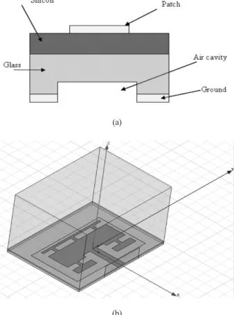
The microstrip antenna was designed on a silicon substrate in order to improve the integrated sensor characteristics on the same substrate. High index substrate materials, such as Si(ε= 11.9), enable a smaller overall circuit and antenna size, however it is easy to excite surface waves which result in a reduced bandwidth and a degradation in radiation efficiency. This problem was solved by using micromachining technology, which is able to synthesize silicon substrates with a low index or an air cavity[8]. The simulated structure of the antenna is shown in Fig. 1. The relative dielectric constant of the multilayer can be written as [8]:
where hn and εn are the thickness and the relative dielectric constant of the nth dielectric layer, respectively.
With the silicon substrate at h1= 0.5 mm, ε1= 11.9 and the glass substrate at h2= 1 mm, ε2 = 4.6, the equivalent permittivity of the silicon/glass substrate was estimated to be εr= 5.8 by using (1).
One drawback found in the silicon substrate in the microstrip antenna is a loss on the substrate caused by the silicon conductivity. This can be reduced by using high resistivity silicon(HRS) or a thin insulator material SiO2 [9]. Therefore, the microstrip patch antenna was designed on a HRS/glass substrate. These substrates are bonded easily using high quality anodic bonding; this structure can operate stably at high frequencies. The operating frequency depends mainly on the patch geometry and the dielectric constant of the substrate. A back air cavity was etched into the glass substrate in order to enhance the performance of the antenna and also to control the resonant frequency slightly. The size of the patch can be determined by (1) and by (2)-(5) and are denoted in Fig. 2[10].
The dimensions of the proposed antenna were calculated for a frequency of 2.4 GHz. The end results from (1)-(5) were : ε= 5.8, W = 34 mm and L = 26 mm. The antenna feed needs to be designed carefully since it must provide a correct impedance matching. At high-signal frequencies it is necessary to design a feed-line with a specific characteristic impedance. Also, the line must be connected to a point in the antenna where the input impedance is the same as the feed-line impedance. The patch antenna was fed using a microstrip line connected to a point inside the
Fig. 1. (a) The cross-view and (b) the antenna structure designed using HFSS.
(b)
(1) (2)
(3)
(4)
(5)
(a)
Fig. 2 The basic parameters for the inset-fed patch antenna.
patch where the input impedance is 50 Ω. In this simulation, the inset-fed length of yo = 8.75 mm was calculated using equations from [11]. The patch dimensions and the inset-fed length were then adjusted and optimized through simulation. The overall reconfigurable antenna was design by following these steps : (a) design and optimize the antenna at 2.4 GHz, as seen in Table 1, (b) cut-out the patch antenna geometry and control the inset-fed length in order to obtain the best structure at 5.7 GHz, as seen in Table 1, (c) replace the metal lines at the switch positions and consider the effects of electromagnetic fields on the patch when the switches are present, (d) re- adjust the patch antenna dimensions.
3. THE RESULTS AND DISCUSSIONS
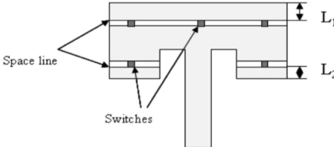
On the patch metal, which was designed to resonate at 2.4 GHz using the parameters from Table 1, we used a space line cut-out in the metal patch, as shown in Fig. 3.
The width of the space line was sufficient to eliminate the electromagnetic effects from the other parts of the patch;
this distance must be larger than ΔL = 0.7 mm, as calculated by (4). This value was investigated by simulation and the best value was found to be 2.6 mm. Fig.
4 shows the geometry of the antenna operated at 5.7 GHz, which was separated from the 2.4 GHz antenna geometry by the space line.
The position of the space lines were gradually shifted to the center of patch until the antenna resonated in a range from 5.7 to 5.8 GHz. At the resonant frequency of 5.74 GHz the return loss was -30 dB, the -10 dB band width was 180 MHz with a gain 8 dB. These simulation results are shown in Fig. 5(a) and 5(b).
Fig. 5. (a) The return loss and (b) the antenna gain at 5.7 GHz with the five switches in the OFF state.
(b) (a)
Fig. 4. The distribution of surface current J on the metal patch at 5.7 GHz.
Fig. 3. The optimized patch antenna and switches.
Table. 1. The antenna dimensions Parameter Dimensions at 2.4
GHz(mm)
Dimensions at 5.7 GHz(mm) Patch metal,
L × W Silicon substrate,
L × W × h Glass substrate,
L × W × h Air cavity, L × W × h Length of inset line
section yo Width of inset slot line
section Wf Length of feed
line Lf Width of feed line Wf
26 × 34
37 × 50 × 0.5
37 × 50 × 1
24 × 40 × 0.08
8
4
7
4
10 x 34
37 x 50 x 0.5
37 x 50 x 1
24 x 40 x 0.08
1.6
4
13
4
Five 2.6×1.5 mm2metal jumpers were substituted for the switches used to connect the patches. The presence of the jumpers and the space lines changed the resonant frequency of the antenna to 2.4 GHz; the values L1and L2 (marked in Fig. 3) were again optimized. The results seen in Fig. 6 show the highest return loss of the antenna occurs when L1= 1 mm and L2 = 3 mm. Fig. 7 shows that the antenna resonated at 2.42 GHz with a return loss -15 dB, the simulated bandwidth and gain were measured at 20 MHz and 1 dB, respectively(with L1= 1 mm, L2= 3 mm).
The narrower bandwidth of the antenna at 2.4 GHz may be caused by the sub patches, which are connected to each other via metal lines(switches in the ON state). This non- continuous metal patch reduced the radiation efficiency of the patch antenna.
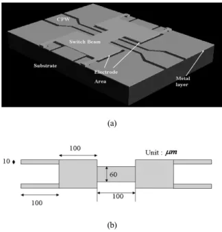
The replacement of the five metal jumpers with MEMS switches was performed next. The 2.6×1.5 mm2area was
reconstructed, which became a coplanar waveguide with an overlaying metal beam, as seen in Fig. 8(a). The calculation for the permittivity of the silicon/glass resulted in an εr = 5.8, a coplanar waveguide(CPW) center conductor width of w = 50 μm and a ground spacing of s = 10 μm[12]. A CPW with a 40 μm separation was used in this design. The RF MEMS switches integrated into the reconfigurable antenna must be well isolated at 5.7 GHz and have a good conduction at 2.4 GHz during the OFF and ON states, respectively. The membrane was made from gold because it possesses a low Young’s modulus, is flexible, and has a high conductivity. The shape and size of the membrane are shown in Fig. 8(b). The RF MEMS DC contact switches were designed and analysed using ANSYS software; some basic parameter are given in Table 2.
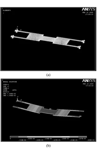
The 2 μm thick membrane was suspended 3 μm above the substrate in order to obtain a good isolation; in this simulation Solid 185 was chosen as the meshing membrane element type. Two electrostatic forces were generated by DC voltage on two electrodes. In the simulation, they were placed at the center of the electrodes as a constant force, as shown in Fig. 9(a). The spring constant of this structure was measured at k = 38 N/m by ANSYS; the force needed to displace the area contact on the membrane by 3 μm was F = k.x = 38×3×10-6= 114 μ N. The DC voltage needed to actuate this switch is shown in the figure, taken from [13]; it was determined to be 58.6V. The 3 μm displacement of membrane in the simulation is shown in Fig. 9(b).
Fig. 6. The return loss when the length of L1varies from 1 mm to 5 mm with L2fixed at 3 mm.
Fig. 7. (a) The return loss and (b) the gain of the antenna at 2.4 GHz (the five switches in the ON state).
(b) (a)
Fig. 8 (a) The MEMS switch structure and (b) dimensions.
(b) (a)
4. CONCLUSION
This paper presented the design for a reconfigurable microstrip patch antenna. By controlling the bias DC
voltage applied to MEMS switches, the antenna can be switched between 5.7 GHz at 0 V to 2.4 GHz at 58.6 V.
The design antenna has the high gains of 8 dB and 1 dB at 5.7 GHz and 2.4 GHz, respectively. The high gain antenna will enhance the communication distance of a sensor in a wireless sensor node. The antenna, placed on a silicon substrate, is easy to integrate with MEMS switches or other components on the same substrate. The tunable antenna using different ISM bands will improve the flexibility of a sensor in a wireless sensor system.
ACKNOWLEDGMENT
This research was supported by a Korean Research Foundation Grant through the Human Resource Training Project for Regional Innovation funded in 2010 by the Korean Government which was conducted by the Ministry of Education, Science and Technology.
REFERENCES
[1] P. M. Mendes, M. Bartek, J. N. Burghartz, and J. H.
Correia, “Novel very small dual-band chip size antenna for wireless sensor networks”, Proc. IEEE RAWCON, pp. 419-422, Atlanta, USA, 2004.
[2] P. M. Mendes, A. Polyakov, M. Bartek, J. N.
Burghartz, and J. H. Correia “Integrated 5.7 GHz chip size antenna for wireless sensor network”, Transducers’03, pp. 49-52, Boston, USA, 2003.
[3] W.-S. Yoon, S.-M. Han, D.-H. Lee, K.-J. Lee, S. Pyo, and Y.-S. Kim, “A reconfigurable circularly polarized microstrip antenna on a cross-shape slotted ground”, Journal of the Korea Electromagnetic Engineering Society, vol. 21, no. 1, pp. 46-52, 2010.
[4] M. Maddela, R. Ramadoss, and R. Lempkowski, “A MEMS-based tunable coplanar patch antenna fabricated using PCB processing techniques”, Journal of Micromech. and Microeng., vol. 17, pp. 812-819, 2007.
[5] R. N. Simons, D. Chun, and L. P. B Katehi,
“Microelectromechanical systems(MEMS) actuators for antenna reconfigurability”, NASA Research Report, NASA CR-2001-210612, 2001.
[6] K. Topalli, O. A. Civi, S. Demir, S. Koc, and T. Akin,
“Dual-frequency reconfigurable slot dipole array with a CPW-based feed network using RF MEMS technology for X-and Ka band application”, Antennas and
(a)
Fig. 9. (a) The modeling and (b) the 3 μm deformation of the membrane.
(b)
Table. 2. The DC contact MEMS switch parameters
Parameter Value
Length [μm]
Width [μm]
Height [μm]
Membrane type Thickness [μm]
Actuation area [μm2] Actuation voltage [V]
500 100 3 Gold
2 100×100(×2)
58.6
Propagation International Symposium, ISBN: 978-1- 4244-0877-1, pp. 825-828, 2007.
[7] P. Blondy, D. Bouyge, A. Crunteanu, and A. Pothier,
“A wide tuning range MEMS switched patch antenna”, Microwave Symposium Digest, IEEE MTT-S International, pp. 152-154, 2006.
[8] W. Pan, S.-Z. Wu, and Y. Chen, “Micromachined patch antennas on synthesized substrates”, International Conference on Mirowave and Milimeter Wave Technology Proceedings, pp. 58-61, 2004.
[9] P. Sharma, S. K. Koul, and S. Chandra, “Micromachin- ed inset-fed patch antenna at Ka-band”, Proceedings of Asia Microwave Pacific Conference(APMC-2006), pp.
12-15, Yokohama, Japan, 2006.
[10] H. Fang, Z. Jian, Y. Yuan-wei, and W. Jing,
“Milimeter-wave design of aperture-coupled micromachined patch antennas”, ICMMT 2008 Proceedings, pp. 1401-1404, April 2008.
[11] Design Inset-Fed Microstrip Patch Antenna, www.mwrf.com.
[12] Coplanar wave guide calculator, www.micro- waves101.com.
[13] Gabriel M. Rebeiz, RF MEMS theory, design, and technology, John Wiley & Son, ISBN: 0-471-20169-3, p. 38.
Phan Duy Thach received his B.E.
degree at the School of Electrical Engineering, Ho Chi Minh University of Technology, Ho Chi Minh, Vietnam, in 2008, and an M.E. degree at the School of Electrical Engineering, University of Ulsan, Ulsan, South Korea, in 2010. He is now working as a Ph.D candidate at the School of Electrical Engineering, University of Ulsan, Ulsan, South Korea. His research interests include SAW sensors based ZnO/AlN thin films, MEMS, antennas and FEM modeling.
Gwiy-Sang Chung received his B.E.
and M.E. degrees in Electronic Engineering from Youngman Univer- sity, Kyongsan, South Korea, in 1983 and 1985, respectively, and his Ph.D.
degree from Toyohashi Universty of Technology, Toyohashi, Japan, in 1992.
He joined ETRI, Daejon, South Korea, in 1992, where he worked on Si-on- insulator materials and devices. In addition, he has worked as a visiting scholar at UC Berkeley, Stanford University., CA, USA, in 2004 and 2009, respectively. He is now a professor at the School of Electrical Engineering, University of Ulsan, Ulsan, South Korea. His research interests include SiC, ZnO, AlN- M/NEMS, wireless sensor nodes energy harvesting and graphene.