• 검색 결과가 없습니다.

Deposition Optimization and Property Characterization of Copper-Oxide Thin Films Prepared by Reactive Sputtering

N/A
N/A
Protected

Academic year: 2021

Share "Deposition Optimization and Property Characterization of Copper-Oxide Thin Films Prepared by Reactive Sputtering"

Copied!
5
0
0

로드 중.... (전체 텍스트 보기)

전체 글

(1)

Deposition Optimization and Property Characterization of Copper-Oxide Thin Films Prepared by Reactive Sputtering

Yil-Hwan You, Seung-Muk Bae, Young-Hwan Kim and Jinha Hwang

Dept. of Mat. Sci. & Eng., Hongik Univeristy, Seoul 121-791, KOREA (Received March 19, 2013: Corrected March 28, 2013: Accepted March 29, 2013)

Abstract: Copper-oxide (CuO) thin films were prepared by reactive sputtering of Cu onto Si wafers and characterized using a statistical design of experiments approach. The most significant factor in controlling the electrical resistivity and deposition rate was determined to be the O
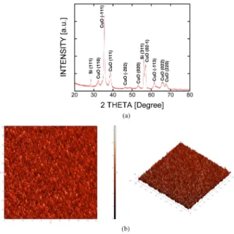
2

fraction. The deposited CuO thin films were characterized in terms of their physical and chemical properties, using X-ray photoelectron spectroscopy (XPS), atomic force microscopy (AFM), X- ray diffraction (XRD), and 4-point resistance measurements. The deposited copper thin films were characterized by XPS and XRD analyses to consist of Cu

2+

. The CuO thin films of highest resistivity exhibited superior rectifying responses with regard to n-type Si wafers, with a current ratio of 3.8 ×10

3

. These superior responses are believed to be associated with the formation of a charge-depletion region originating from the p-type CuO and n-type Si materials.

Keywords: CuO thin films, Nonohmic Responses, Diode, n-Type Si

1. Introduction

Copper oxide is a semiconducting oxide of p-type characteristics, along with another transition metal oxide, NiO. Its major defects are known to be metal deficiencies, i.e., copper vacancies, and such unique features allow the use of copper oxide in photoelectrochemical, photovoltaic, and gas-sensing applications.

1-4)

With the combination of other n-type materials, high-performance diode devices have been gaining academic and industrial attention as switching elements in nonvolatile memories, which are equivalent to switching transistors in information display panels such as TFT LCDs.

5-6)

Copper oxide exists as either CuO or Cu

2

O, and the corresponding bandgaps and crystalline structures differ significantly.

7-9)

Copper oxide can be prepared using a variety of techniques such as thermal oxidation, electrodeposi- tion, chemical deposition, reactive sputtering, molecular epitaxy, and cyclic chemical vapor deposition.

10-15)

The majority of research on functional oxides has been limited to oxide-based thin films transistors (TFTs) and non-volatile memories.

16-18)

Such extensive attention in academia and industry has resulted in the commercialization of transparent conducting oxides and the novel development and applications of high-performance oxide-based transistors to

replace the pre-existing amorphous Si-based TFTs.

Copper oxide shows resistive switching responses in unipolar and bipolar modes.

19-20)

Furthermore, the CuO/

InZnO

x

multilayered nanostructure exhibits superior device performance applicable to resistive switching elements, along with rectifying diodes with a current ratio on the order of 10

5

.

20)

The multiple functions of copper oxide are related to its defect chemistry and its modification through the involvement of metal deficiencies in the form of copper vacancies.

21)

In addition, before the current attention to diodes as switching elements, CuO thin films were combined with n- type materials for use of the heterojunction in gas-sensing applications.
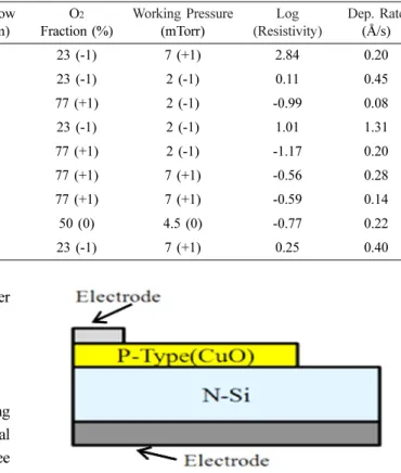
3)

The current work reports an experimental approach to the optimization of CuO thin films, and proposes the fabrication of p-type CuO thin films on n-type Si wafers, with the aim of developing a rectifying diode. In order to trace the physical/chemical features in copper oxides, the thin-film deposition procedure was investigated using a statistical design of experiments (DoE) approach.

21)

The screened copper oxides were proposed as input materials for the diode applications. The deposited copper oxides were characterized in terms of their physical and chemical properties, including their electrical and structural aspects in addition to the

Corresponding author

E-mail: [email protected]

© 2013, The Korean Microelectronics and Packaging Society

This is an Open-Access article distributed under the terms of the Creative Commons Attribution Non-Commercial License(http://creativecommons.org/

licenses/by-nc/3.0) which permits unrestricted non-commercial use, distribution, and reproduction in any medium, provided the original work is

properly cited.

(2)

chemical states of the copper cations in the binary copper oxides.

2. Experimental Procedure

For the determination of the effects of the processing variables on the deposition of CuO thin films, a statistical DoE was applied to the reactive sputtering of CuO. Three variables were chosen: the RF power, the relative fraction of O

2

/Ar, and the working pressure. The output variables were chosen to be the deposition rate and the logarithmical value of resistivity. In terms of the processing conditions, the RF power was controlled between 100 and 50 W for the high and low levels, denoted by (+1) and (–1), respectively, the O

2

fraction was varied between 23% and 77%, and the working pressure was varied between 7 and 2.5 mTorr. The DoE included one center point. The copper target employed had a purity of 99.99%. The base pressure was maintained at approximately 2 ×10

-6

Torr. The designed runs are shown in Table 1, along with the output information. Before the deposition of the CuO thin films, the highly doped Si wafers were cleaned thoroughly using acetone, methanol, and deionized water.

The chemical state of the deposited CuO thin films was characterized using X-ray photoelectron spectroscopy (XPS), the surface morphology was probed using atomic force microscopy (AFM), the electrical properties were analyzed through four-point resistance measurements, and crystal-structure information was obtained through high- resolution X-ray diffraction (XRD) analysis. The electrical characterization was performed in the two-point electrode configuration, as shown in Fig. 1. The CuO thin films were deposited with a thickness of 60 nm onto highly doped n- type Si wafers. The top electrode was deposited onto the CuO thin film using a Pt target. Disc-shaped Pt patterns

were fabricated using a metal shadow mask, and the diameter of the Pt electrode was controlled to be approximately 160 µm. The bottom electrode of the n-type Si wafer was prepared using a silver paste followed by ambient heating at 100

o

C. The current–voltage characteristics of the CuO/Si diode were measured using a semiconductor parameter analyzer (4156C, Agilent, Palo-Alto, USA). The current levels were measured between –2.5 and +2.5 V.

3. Results and Discussion

As summarized in Table 1, the copper oxides were monitored using an experimental design based on statistical full-factorial design, where three factors were employed at two levels, i.e., the high and low levels denoted by (+1) and (–1), respectively. As summarized in Tables 2 and 3, the experimental variable, i.e., the O

2

fraction (O

2

/Ar), was determined to be a major variable, controlling the electrical resistivity in a logarithmic manner. The deposition rate was affected significantly by the O

2

fraction but to a much smaller extent by the RF power and the working pressure.

In addition, the interaction of the RF power and working Table 1. Nine-run experimental design for studying the effects of RF power, O

2

fraction, and working pressures on the logarithmic value

of resistivity and deposition rates of copper oxide thin films prepared through reactive sputtering.

Standard Order

Run Order

Center Point

RF Power (W)

Ar Flow (sccm)

O

2

Flow (sccm)

O

2

Fraction (%)

Working Pressure (mTorr)

Log (Resistivity)

Dep. Rate (Å/s)

5 1 1 50 (-1) 10 3 23 (-1) 7 (+1) 2.84 0.20

1 2 1 50 (-1) 10 3 23 (-1) 2 (-1) 0.11 0.45

3 3 1 50 (-1) 3 10 77 (+1) 2 (-1) -0.99 0.08

2 4 1 100 (+1) 10 3 23 (-1) 2 (-1) 1.01 1.31

4 5 1 100 (+1) 3 10 77 (+1) 2 (-1) -1.17 0.20

8 6 1 100 (+1) 3 10 77 (+1) 7 (+1) -0.56 0.28

7 7 1 50 (-1) 3 10 77 (+1) 7 (+1) -0.59 0.14

9 8 0 75 (0) 7 6 50 (0) 4.5 (0) -0.77 0.22

6 9 1 100 (+1) 10 3 23 (-1) 7 (+1) 0.25 0.40

Fig. 1. Device structure employed for the electrical characterization

of rectifying diodes involving CuO thin films on n-type Si

wafers.

(3)

pressure affected the overall deposition rate. The O

2

fraction played dominant roles in terms of both the resistivity and deposition rate: a high O

2

fraction led to a slower deposition rate and lower resistance, and a low O

2

fraction resulted in a higher deposition rate and higher resistance in the CuO thin films. From the results summarized in Table 1, two extreme cases of CuO thin films were chosen for further characterization as active devices.

From Run No. 5, the combination of a high RF power, high O

2

fraction, and low working pressure induced the lowest resistivity of 6.73×10

-2

Ω·cm in the CuO thin films.

In contrast, the combination of a low RF power, low O

2

fraction, and high working pressure resulted in the CuO thin film with the highest resistivity of 698 Ω·cm. However, these two sets of conditions did not show any difference in deposition rate.

The XRD results for the copper oxides are shown in Fig.

2(a). The peak indexing allows for the formation of CuO rather than Cu

2

O. The surface morphology was monitored using AFM on the CuO thin films (see Fig. 2(b)). The CuO with the highest resistivity exhibited a surface roughness of 0.49 nm, suggesting indirectly that the rather high roughness reflects the crystalline features formed on the top surface of the CuO thin films.

The XPS results in Fig. 3 show two main peaks followed

by the corresponding satellite peaks. The core peaks are found to be at 933.72 and 953.52 eV for Cu 2p

1/2

and Cu 2p

3/2

, respectively, and the two satellite peaks are at 945.02 and 963.72 eV, respectively. The positions of the core peaks and the presence of the two satellite peaks support the presence of CuO rather than Cu

2

O, i.e., the formation of CuO with Cu in the +2 valence state.

Among the conditions proposed through the DoE, two extreme cases were chosen for diode fabrication: the one Table 2. Calculated effects for the logarithmic value of resistivity

of copper oxide thin films.

Term Effect Coefficient

Constant   0.11

RF Power -0.46 -0.23

O2 Fraction -1.88 -0.94

Working Pressure 0.75 0.37

RF Power*O2 Fraction 0.38 0.19

RF Power*Working Pressure -0.82 -0.41

O2 Fraction*Working Pressure -0.24 -0.12 RF Power*O2 Fraction*Working Pressure 0.92 0.46

Table 3. Calculated effects for deposition rate of copper oxide thin films.

Term Effect Coefficient

Constant   0.38

RF Power 0.33 0.17

O2 Fraction -0.42 -0.21

Working Pressure -0.25 -0.13

RF Power*O2 Fraction -0.20 -0.10

RF Power*Working Pressure -0.16 -0.08

O2 Fraction*Working Pressure 0.33 0.16

RF Power*O2 Fraction*Working Pressure 0.17 0.08

Fig. 2. (a) High-resolution X-ray diffraction obtained from copper oxide thin films of highest resistivity. (b) AFM Images scanned 1 µm×1 µm of CuO thin films showing highest resistivity.

Fig. 3. XPS survey results on copper oxide thin films of highest

resistivity prepared through reactive sputtering. (a) survey

spectrum, (b) Cu 2p core spectrum, and (c) O 1s core peaks

spectra.

(4)

with the highest resistivity (698 Ω·cm) and that with the lowest resistivity (6.73 ×10

-2

Ω·cm). As shown in Fig. 4, the two copper oxides exhibit rectifying results in the diode structure where n-type Si is employed as a substrate for the p-type CuO thin films. Considering the magnitude of the resistivity, the charge-carrier concentrations are expected to be below 10

17

/cm

3

. The expected charge-carrier concentra- tion is much smaller than the electronic concentration present in N+Si wafers (approximately 10

20

/cm

3

). As shown in Fig. 4, the reverse and forward currents show rectifying responses in the as-deposited states. The CuO thin film with the highest resistivity exhibits a reverse current of 2.17×10

-7

A at –2.5 V and a forward current of 8.28 ×10

-4

A at +2.5 V, with a current ratio of 3.8×10

3

. On the other hand, the CuO thin film with the lowest resistivity shows a reverse current of 1.91×10

-5

A and a forward current of 1.43×10

-4

A, with a current ratio of 7.5. However, both CuO thin films have similar on-voltages of around 1.5 V. In other words, the highest resistance is appropriate for the formation of high- performance nano-diodes on Si wafers. The current device construction is based on the different conduction band offsets and valence band offsets. Such imbalance leads to the formation of a potential barrier in the reverse applied voltages.

The current work reports a preliminary result that includes the deposition optimization of CuO thin films with special

emphasis on their electrical resistivity. Through combination with n-type Si wafers, the p-type CuO thin films demonstrated device integration with the high rectifying performance required of switching-functioning elements. Additional device optimization will be reported in combination with the sophisticated control of the physical and chemical properties of p-type conducting copper oxides.

4. Conclusions

p-Type CuO thin films were prepared on Si wafers using reactive sputtering of Cu targets with oxygen/argon mixtures. The most significant variables were determined to O

2

fraction. The copper oxides were found to be crystalline, p-type conducting oxides. The valence state of Cu was found to be +2, leading to the formation of CuO. The integration of CuO on n-type Si wafers results in rectifying behavior in the diodes. In particular, the CuO thin films with the highest resistivity gave rise to the highest rectifying behaviors in the devices constructed on n-type Si wafers.

Such a diode performance is attributed to the difference in the conduction band and valence band offsets imparted by the p-type CuO thin film and the n-type Si wafer.

Acknowledgements

This research was supported by Basic Science Research Program through the National Research Foundation of Korea (NRF) funded by the Ministry of Education, Science and Technology (NRF-2010-0009179).

References

1. Y. S. Chaudhary, A. Agrawal, R. Shrivastav, V. R. Satsangi, and S. Dass, “A Study on the Photoelectrochemical Properties of Copper Oxide Thin Films”, Int. J. of Hydrogen Energy, 29, 131 (2004).

2. Q. Bao, C. M. Li, L. Liao, H. Yang, W. Wang, C. Ke, Q.

Song, H. Bao, T. Yu, K. P. Loh, and J. Guo, “Electrical Trans- port and Photovoltaic Effects of Core-Shell CuO/C

60

Nanow- ire Heterostructure”, Nanotechnology, 20, 065203 (2009).

3. Y. Ushio, M. Miyayama, and H. Yanagida, “Effects of Inter- face States on Gas-Sensing Properties of a CuO/ZnO Thin- Film Heterojunction”, Sens. Actuators, B 17, 221 (1994).

4. P. Samarasekara, N. T. R. N. Kumara, and N. U. S. Yapa, J.

Phys. : Condens. Matter 18, 2417 (2006).

5. B. S. Kang, S.-E. Ahn, M.-J. Lee, G. Stefanovich, K. H. Kim, W. X. Xianyu, C. B. Lee, Y. Park, I. G. Baek, and B. H. Park,

“High-Current-Density CuO

x

/InZnO

x

Thin-Film Diodes for Cross-Point Memory Applications”, Adv. Mater., 20, 3066 (2008).

6. M.-J. Lee, S. I. Kim, C. B. Lee, H. Yin, S.-E. Ahn, B. S.

Kang, K. H. Kim, J. C. Park, C. J. Kim, I. Song, S. W. Kim, Fig. 4. Current(I)-voltage(V) characteristics: (a) and (b) I-V informa-

tion obtained from CuO thin films of highest resistivity ((a):

linear scale, (b): semi-logarithmic scale), and (c) and (d) I-V

information obtained CuO thin films of lowest resistivity

CuO ((c): linear scale, (d): semi-logarithmic scale).

(5)

G. Stefanovich, J. H. Lee, S. J. Chung, Y. H. Kim, and Y.

Park, “Low-Temperature-Grown Transition Metal Oxide Based Storage Materials and Oxide Transistors for High-Den- sity Non-volatile Memory”, Adv. Funct. Mater., 19, 1587 (2009).

7. F. Marabelli, G. B. Parraviciny, and F. S. Drioli, “Optical Gap of CuO”, Phys. Rev. B, 52, 1433 (1995).

8. J. Ghijsen, L. H. Tjeng, J. V. Elp, H. Eskes, J. Westerink, G.

A. Sawatzky, and M. T. Czyzyk, “Electronic Structure of Cu

2

O and CuO”, Phys. Rev. B, 38, 11322 (1988).

9. B. P. Rai, “Cu

2

O Solar Cells. A Review”, Sol. Cells, 25, 265 (1988).

10. J. B. Liang, N. Kishi, T. Soga, T. Jimbo, and M. Ahmed,

“Thin Cuprous Oxide Films Prepared by Thermal Oxidation of Copper Foils with Water Vapor”, Thin Solid Films, 520, 2679 (2012).

11. J. Morales, L. Sa´nchez, S. Bijani, L. Martý´nez, M. Gaba´s, and J. R. Ramos-Barrado, “Electrodeposition of Cu

2

O: An Excellent Method for Obtaining Films of Controlled Mor- phology and Good Performance in Li-Ion Batteries”, Electro.

Solid-state Lett., 8, A159 (2005).

12. J. Pinkas, J. C. Huffman, D. V. Baxter, M. H. Chisholm, and K.

G. Caulton, “Mechanistic Role of H

2

O and the Ligand in the Chemical Vapor Deposition of Cu, Cu

2

O, CuO, and Cu

3

N from Bis(1,1,1,5,5,5-hexafluoropentane-2,4-dionato)copper(II)”, Chem. Mater., 7, 1589 (1995).

13. K. Kawaguchi, R. Kita, M. Nishiyama, and T. Morishita,

“Molecular Beam Epitaxy growth of CuO and Cu

2

O Films

with Controlling the Oxygen Content by the Flux Ratio of Cu/

O”, J. Cryst. Growth, 143, 221 (1994).

14. V. F. Drobny, and D. L. Pulfrey, “Properties of Reactively- Sputtered Copper Oxide Thin Films”, Thin Solid Films, 61, 89 (1979).

15. M. K. Kim and Jinha Hwang, in Preparation.

16. K. Nomura, H. Ohta, A. Takagi, T. Kamiya, M. Hirano, and H. Hosono, “Room-Temperature Fabrication of Transparent Flexible Thin-Film Transistors Using Amorphous Oxide Semiconductors”, Nature, 432, 488 (2004).

17. C.-S. Park, “Electrical Characteristics of (BaSr)TiO

3

/RuO

2

Thin Films”, J. Microelectron. Packag. Soc., 11(3), 63 (2004).

18. I.-S. Park, K.-R. Kim, and J. An, “Resistance Switching Char- acteristics of Binary SiO

2

and TiO

2

Films”, J. Microelectron.

Packag. Soc., 13(2), 15 (2006).

19. P. Zhou, M. Yin, H. J. Wan, H. B. Lu, T. A. Tang, and Y. Y.

Lin, “Role of TaON Interface for Cu

x

O Resistive Switching Memory Based on a Combined Model”, Appl. Phys. Lett., 94, 053510 (2009).

20. H. B. Lv, M. Yin, X. F. Fu, Y. L. Song, L. Tang, P. Zhou, T.

A. Tang, B. A. Chen, and Y. Y. Lin, “Resistive Memory Switching of Cu

x

O Films for a Nonvolatile Memory Appli- cation”, IEEE Electron Device Lett., 29, 309 (2008).

21. G. E. P. Box, J. S. Hunter, W. G. Hunter, Statistics for Exper- imenters: Design, Innovation, and Discovery, 2nd ed., pp.

235-279, A John Wiley & Sons, Inc., Hoboken, New Jersey

(2005).

수치

Fig. 1. Device structure employed for the electrical characterization of rectifying diodes involving CuO thin films on n-type Si wafers.
Table 3. Calculated effects for deposition rate of copper oxide thin films.

참조

관련 문서

The pulses generate an electrochemical reaction, inducing nanoscale silicon oxide deposits on the wafer surface.. This research focused on variations in

The Study on the Changes of Bacterial Inorganic Phosphate Metabolism in Interactions between Nitric Oxide and Salmonlla enterica serovar Typhimurium..

a second phase forms because of the limited solubility of zinc in

pottery, tableware, cookware, building materials, aerospace materials, to nuclear materials (e.g., UO 2 pellets, waste forms, etc.)... A’ a’ B’ b’ C’

Decomposition (MOD) process, and then the zinc oxide nanorods on ZnO seed layer were grown by hydrothermal process from 0.3 M at pH 7, 80 ℃ , 1 h. Single phase zinc oxide

Improvement of the Performance and Stability of Oxide Semiconductor Thin-Film Transistors Using Double-Stacked Active Layers.. Metal oxide semiconductor

Laser-induced doping of amorphous copper diselenide (α-CuSe 2 ) thin film with gallium (Ga) and indium (In) was performed to control/improve their electrical

Among the various methods, plasma electrolytic oxidation (PEO) is a method for surface processing in which a biocompatible oxide film is formed using a number of ions..