韓國電磁波學會論文誌 第21 卷 第 10號 2010年 10月 論文2010-21-10-03
. 서 론
[1]
[9]
.
[1],[2]
,
[3],[4]
,
[5] [9]
.
,
( ) 3
(4π)
, 2 , 1
2010 .
(Department of Electronics Engineering, Dongseo University)
* (School of Electrical Engineering and Computer Science, Kyungpook National University) : 20100525-068
: (e-mail : [email protected]) : 2010 7 7
Electromagnetic Resonant Transmission through Slits in a Cavity inside Conducting Screen of Finite Thickness
이 종 익 조 영 기 Jong-Ig Lee Young-Ki Cho*
요 약
TE .
,
. 1/ .
.
Abstract
In this paper, the problem of electromagnetic transmission via slits in a cavity inside conducting screen of finite thickness is considered for the case that the TE(to the slit axis) polarized plane wave is incident on the slit in conducting screen. Using the method of moments the variations of the transmitted power through the slits are obtained and compared with those computed from an equivalent circuit constructed using an equivalent slit admittance. It is found that the effective slit width of a narrow slit, at resonance, becomes 1/ wavelengths independently of the actual slit width. The transmission resonance phenomena in the proposed geometry are explained in connection with the variations of an equivalent admittance of the slit in the cavity.
Key words : Cavity, Resonance, Maximum Transmission, Equivalent Admittance, Narrow Slit
(
, )
.
[5],
. 1
.
( ) TE
,
[10]
. , ,
( )
.
.
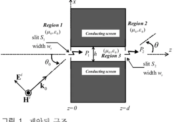
. 이 론
1 d
,
(x=0)
( [5] 1
.).
TE
(
=0) z
,
y 2 ,
(
) .
TM
(1)
,
Region 1
z=0
q0 h
P2 z
Ei
Hi
k0
0 0
( , )m e Conducting screen
Conducting screen 0 0
( , )m e
z=d Region 2
0 0
( , )m e
Region 3 P1
slit 1
width s S
w
slit 2
width s
S w
q
그림 1.
Fig. 1. Geometry under consideration.
,
.
TM (
)
[10] [12]
.
(2-1)
(2-2)
(2-3)
, y
1, 2, 3
(source) . (2-1) (2-3)
(3-1) (3-9) .
(3-1)
′
′ ′
(3-2)
′
′′
(3-3)
′ ′′
′
′
(3-4)
′ ′′
′
′
(3-5)
(4-1)
韓國電磁波學會論文誌 第21 卷 第 10號 2010年10月′′′
∞
․
′
∞
․
′
(3-6)
′′′
∞
․
′
∞
․
′
(3-7)
≧
(3-8)
≧ (3-9)
,
,
′ ′′
,
0 2 Hankel .
S1
[
]
(coupled integral equations)
′ ′′
′′′
′′′
′ ′′
′′′
′′′
(4-2)
[10]
,
′ ′
,
′ ′. (method of moments)
(piecewise constant pulse function) ,
( 10
, .).
3
,
2
S
(Poynting theorem)
×⋅
(5)
.
2
far-field
[W/rad/m)]
.
1
(z
) , y
,
(
).
(effective slit width)
[W/m](
)
[
]
(6)
[11],[12]
.
1 2
[5],[13]
.
d ,
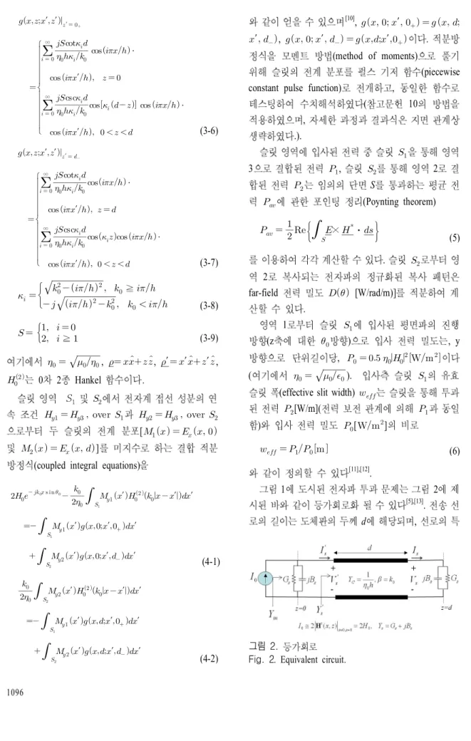
그림 2.
Fig. 2. Equivalent circuit.
h ws
TEM wave
0 z=
Flanged PPW
(a) (a) Structure
YC=1/h0h YS(=GS+jBS)
z=0(slit) gs jbsi jbse 1
yS=YS/YC=gs+jbs
=gs+j(bsi+bse) (b)
(b) Equivalent admittance 그림 3.
[14]
Fig. 3. Equivalent admittance of a slit fed by flanged parallel-plate waveguide[14].
TEM
.
2
3
[14]
. ,
,
2 d=0
′ 2
2 .
120
[14].
(d)
[5],[9]
(7)
2
. 2
, 2
. , 2
′ ′
′′
′
(8) ,
′ 2
(9)
(
) 1
. 1
1
[3],[4]
,
[5]
.
해석 결과 .
3
. 4 [14]
(
) (
)
.
,
,
near-field .
1.0
,
. 0.1
,
韓國電磁波學會論文誌 第21 卷 第 10號 2010年10月
0.001 0.010 0.100 1.000
Waveguide height (h/l0)
0.0 0.5 1.0 1.5 2.0
Normalized admittance ys [=gs+jbs] er=1.0, Xa/l0=0
gs ; a/h=1.0 bsi ; a/h=1.0 bse ; a/h=1.0 gs ; a/h=0.1 bsi ; a/h=0.1 bse ; a/h=0.1 ; / 1.0 ; / 1.0 ; / 1.0 ; / 0.1 ; / 0.1 ; / 0.1
s s
si s
se s
s s
si s
se s
g w h b w h b w h g w h b w h b w h
=
=
=
=
=
=
그림 4. () ()
Fig. 4. Variations of an equivalent admittance against slit width and waveguide height .
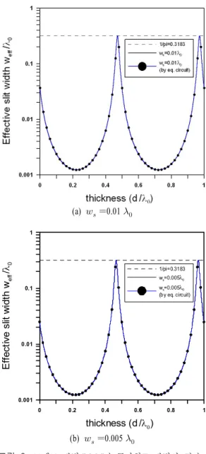
그림 5. . 0.01
Fig. 5. Effects of slit width and conductor thickness.
0.01.
120
=0.1
=1.0
[14]
.
, ,
5
0.01
.
0 .
4
, (7)
.
(a) 0.01
0 0.2 0.4 0.6 0.8 1
thickness (d/l0)
0.001 0.01 0.1 1
Effective slit width weff /l0
1/pi=0.3183 ws=0.005l0 ws=0.005l0 (by eq. circuit)
er1=er2=er3=1.0,h=0.01l0,qi=0
(b) 0.005
그림 6. (MoM)
. 0.01
Fig. 6. Comparison between the results obtained by the method of moments(MoM) and an equivalent circuit approach. 0.01.
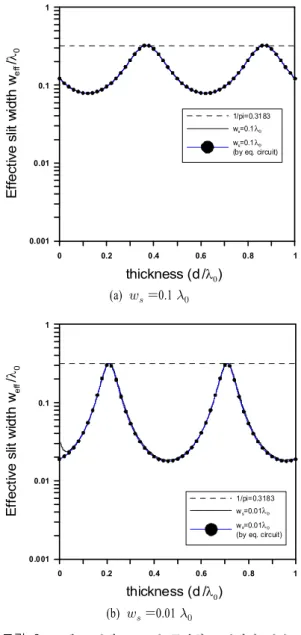
그림 7. . 0.1 Fig. 7. Effects of slit width and conductor thickness.
0.1.
. 6
, 0.01
.
7
0.1
(d)
. 5
. ,
(d) .
8 0.1
,
0.1
d=0
0.01
0.1
d=0
. 4
,
(
) . 6
0 0.2 0.4 0.6 0.8 1
thickness (d/l0)
0.001 0.01 0.1
Effective slit width weff /l0
1/pi=0.3183 ws=0.1l0 ws=0.1l0 (by eq. circuit)
(a) 0.1
0 0.2 0.4 0.6 0.8 1
thickness (d/l0)
0.001 0.01 0.1 1
Effective slit width weff /l0
1/pi=0.3183 ws=0.01l0
ws=0.01l0
(by eq. circuit) er1=er2=er3=1.0,h=0.1l0,qi=0
(b) 0.01
그림 8. (MoM)
. 0.1
Fig. 8. Comparison between the results obtained by MoM and an equivalent circuit approach. 0.1.
(h=0.01
) (
, z )
,
.
(d)
韓國電磁波學會論文誌 第21 卷 第 10號 2010年10月
0 0.2 0.4 0.6 0.8 1
thickness (d/l0)
0.001 0.01 0.1 1
Effective slit width weff /l0
1/pi=0.3183 ws=0.3l0 ws=0.2l0 ws=0.1l0 ws=0.05l0 ws=0.01l0
er1=er2=er3=1.0,h=0.3l0,qi=0
그림 9. . 0.3
Fig. 9. Effects of slit width and conductor thickness.
0.3.
, MoM
.
9
0.3
5 7
.
0.1
0.3
,
0.2
.
10 0.3
,
0.3
d=0
,
0.01
0.1
d=0 .
1
.
0 0.2 0.4 0.6 0.8 1
thickness (d/l0)
0.1 1
Effective slit width weff /l0
1/pi=0.3183 ws=0.3l0 ws=0.3l0 (by eq. circuit)
er1=er2=er3=1.0,h=0.3l0,qi=0
(a) 0.3
0 0.2 0.4 0.6 0.8 1
thickness (d/l0)
0.01 0.1 1
Effective slit width weff /l0
1/pi=0.3183 ws=0.1l0 ws=0.1l0 (by eq. circuit)
er1=er2=er3=1.0,h=0.3l0,qi=0
(b) 0.1
그림 10. (MoM)
. 0.3
Fig. 10. Comparison between the results obtained by MoM and an equivalent circuit approach.
=0.3.
. 결 론
TE
.
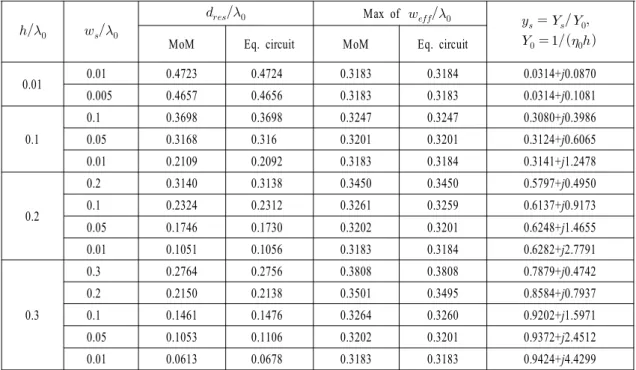
Table 1. Comparison between the results for the resonant length and effective slit width obtained by both the MoM and an equivalent circuit method.
Max of
MoM Eq. circuit MoM Eq. circuit
0.01 0.01 0.4723 0.4724 0.3183 0.3184 0.0314+j0.0870
0.005 0.4657 0.4656 0.3183 0.3183 0.0314+j0.1081
0.1
0.1 0.3698 0.3698 0.3247 0.3247 0.3080+j0.3986
0.05 0.3168 0.316 0.3201 0.3201 0.3124+j0.6065
0.01 0.2109 0.2092 0.3183 0.3184 0.3141+j1.2478
0.2
0.2 0.3140 0.3138 0.3450 0.3450 0.5797+j0.4950
0.1 0.2324 0.2312 0.3261 0.3259 0.6137+j0.9173
0.05 0.1746 0.1730 0.3202 0.3201 0.6248+j1.4655
0.01 0.1051 0.1056 0.3183 0.3184 0.6282+j2.7791
0.3
0.3 0.2764 0.2756 0.3808 0.3808 0.7879+j0.4742
0.2 0.2150 0.2138 0.3501 0.3495 0.8584+j0.7937
0.1 0.1461 0.1476 0.3264 0.3260 0.9202+j1.5971
0.05 0.1053 0.1106 0.3202 0.3201 0.9372+j2.4512
0.01 0.0613 0.0678 0.3183 0.3183 0.9424+j4.4299
,
[
]
. , ,
.
,
,
.
참 고 문 헌
[1] R. F. Harrington, "Resonant behavior of a small aperture backed by a conducting body", IEEE Tr- ans. Antennas Propagat., vol. 30, no. 2, pp. 205- 212, Mar. 1982.
[2] J. -E. Park, J. Yeo, J. -I. Lee, J. -W. Ko, and Y.-K.
Cho, "Resonant transmission of an electrically small aperture with a ridge", J. of Electromagn. Waves and Appl., vol. 23, pp. 1981-1990, 2009.
[3] J. I. Lee, Y. K. Cho, "Electromagnetic transmission through a narrow slit backed by a nearby con- ducting strip", Proc. ISAP05, vol. 3, pp. 1089-1092, Aug. 2005.
[4] Young-Ki Cho, Jong-Ig Lee, and Ki Young Kim,
"On electrical equivalence of aperture-body and tr- ansmission-cavity resonance phenomena in subwa- velength conducting aperture systems from an equi- valent circuit point of view", J. Comput. Theor.
Nanosci., vol. 6, no. 11, pp. 2402-2406, 2009.
[5] R. F. Harrington, D. T. Auckland, "Electromagnetic transmission through narrow slots in thick con- ducting screens", IEEE Trans. Antennas Propagat., vol. AP-28, no. 5, pp. 616-622, Sep. 1980.
[6] Y. Leviatan, R. F. Harrington, and J. R. Mautz,
"Electromagnetic transmission through apertures in
韓國電磁波學會論文誌 第21 卷 第 10號 2010年10月
a cavity in a thick conductor", IEEE Trans. An- tennas Propagat., vol. 30, no. 6, pp. 1153-1165, Nov. 1982.
[7] Y. Takakura, "Optical resonance in a narrow slit in a thick metallic screen", Phys. Rev. Lett., vol. 86, no. 24, pp. 5601-5603, Jun. 2001.
[8] F. Yang, J. R. Sambles, "Resonant transmission of microwaves through a narrow metallic slit", Phys.
Rev. Lett., vol. 89, no. 6, pp. 063901(1)-063901(3), Aug. 2002.
[9] Y. K. Cho, K. W. Kim, J. H. Ko, and J. I. Lee,
"Transmission through a narrow slot in a thick conducting screen", IEEE Trans. Antennas Propa- gat., vol. 57, no. 3, pp. 813-816, Mar. 2009.
[10] D. T. Auckland, R. F. Harrington, "Electromag- netic transmission through a filled slit in a con- ducting plane of finite thickness, TE case", IEEE Trans. Microwave Theory Tech., vol. 26, no. 7,
1992 : (
)
1994 : (
)
1998 : (
) 1998 :
1999 :
주 관심분야
[ ] ,
pp. 499-505, Jul. 1978.
[11] , , "
", , 19(1), p. 120, 2009 11 .
[12] Jong-Ig Lee, Junho Yeo, Jong-Eon Park, and Yo- ung-Ki Cho, "Resonant transmission through slits in a cavity inside thin conducting plane", Proc.
GSMM2010, Incheon, Korea, Apr. 2010.
[13] , , , "
", , 20(1), pp. 83-90, 2009 1 . [14] J. I. Lee, K. W. Kim, and Y. K. Cho, "Equivalent
admittance of a slit fed by a flanged parallel-plate waveguide and maximum coupling mechanism th- rough a narrow slit", JKIEES, vol. 15, no. 11, pp.
1-8, Nov. 2004.
1978 : (
) 1981 :
( )
1998 :
( )
1981 :
2004 2007 : 2008 :
주 관심분야
[ ] , ,
![Fig. 3. Equivalent admittance of a slit fed by flanged parallel-plate waveguide [14]](https://thumb-ap.123doks.com/thumbv2/123dokinfo/5289324.374124/4.892.112.362.86.560/fig-equivalent-admittance-slit-flanged-parallel-plate-waveguide.webp)