ISSN 2288-1069 (Online)
http://dx.doi.org/10.12925/jkocs.2014.31.3.402
Molecular Distribution depending on the Cooling-off Condition in a Solution-Processed
6,13-Bis(triisopropylsilylethynyl)-Pentacene Thin-Film Transistor
Jae-Hoon Park
*․Jin-Hyuk Bae
✝*
Department of Electronic Engineering, Hallym University, Chuncheon 200-702, Korea
✝
School of Electronics Engineering, Kyungpook National University, Daegu 702-701, Korea (Received July 30, 2014; Revised September 15, 2014; Accepted September 17, 2014)
Abstract : Herein, we describe the effect of the cooling-off condition of a solution-processed 6,13-bis(triisopropylsilylethynyl)-pentacene (TIPS-pentacene) film on its molecular distribution and the resultant electrical properties. Since the solvent in a TIPS-pentacene droplet gradually evaporates from the rim to the center exhibiting a radial form of solute, for a quenched case, domains of the TIPS-pentacene film are aboriginally spread showing original features of radial shape due to suppressed molecular rearrangement during the momentary cooling period. For the slowly cooled case, however, TIPS-pentacene molecules are randomly rearranged during the long cooling period. As a result, in the lopsided electrodes structure proposed in this work, the charge transport generates more effectively under the case for radial distribution induced by the quenching technique. It was found that the molecular redistribution during the cooling-period plays an important role on the magnitude of the mobility in a solution-processed organic transistor. This work provides at least a scientific basis between the molecular distribution and electrical properties in solution-processed organic devices.
Keywords : TIPS-pentacene, organic thin-film transistor, cooling-off, molecular distribution, solution-process.
1. INTRODUCTION
Recently, organic semiconductor materials have been attracting much attention due to their potential for flexible electronic devices such as portable displays, disposable sensors, and smart cards [1-4]. Since the transistor is the core and basic element for organizing electronic products, many researchers have
✝
Corresponding author (E-mail: [email protected])
preferentially studied transistors that use
organic semiconductors. Among the many
techniques for fabricating organic thin-film
transistors (OTFTs), solution-processes such as
spin-coating, dip-coating, and ink-jet printing
have been receiving great attention in the last
few decades because of comparative advantages
such as desirable large-area applicability and
cost-effective fabrication [5,6]. However,
relatively low electrical properties in
solution-processed OTFTs have been a kind of
barrier for their practical application [7,8].
In order to enhance the electrical properties in solution-processed OTFTs, many efforts have been devoted to obtaining aligned features of solution-processed organic semiconductor molecules because charge transport is strongly governed by the distributed states of the molecules [9-12].
Previously, in order to obtain ordered features in solution-processed organic semiconductor molecules for better electrical properties in OTFTs, the gradual solvent evaporating method [9], solution-sheared deposition [10], and pinning a droplet on a tiled substrate [11]
have been successfully demonstrated. However, such approaches focus on molecular alignment during the solvent evaporation step. No attempt has been made to examine how the molecules are affected during the cooling-off step carried out after the solvent evaporation step which has been explored so far.
In this work, we studied the effect of the cooling-off conditions on the molecular distribution of solution-processed organic semiconductors, 6,13-bis(triisopropylsilylethynyl) pentacene (TIPS-pentacene) and its resultant electrical properties in the TIPS-pentacene TFTs. When the TIPS-pentacene film was cooled slowly, the TIPS-pentacene molecules exhibited a randomly distributed shape breaking the radial distribution which occurs naturally at the solvent evaporation stage before the cooling-off step. This is attributed to the TIPS-pentacene molecules which are rearranged due to the thermal energy during the relatively long cooling-off time. However, when the TIPS-pentacene film was quenched to room temperature, the domains of TIPS-pentacene remains same showing a radial distribution due to the short period of time to be rearranged. Consequently, the electrical properties are significantly affected in our solution-processed OTFTs according to the cooling-off conditions. This suggests that the cooling-off condition of solution-processed organic semiconductor films have an important role on the capability of the charge transport
in solution-processed OTFTs.
2. EXPERIMENTAL PROCEDURE Figure 1(a) shows a cross-sectional schematic diagram of a top contact TIPS-pentacene TFT. As a gate electrode, a heavily doped p type silicon was used. A 300 nm thick silicon dioxide film was used as a gate insulator layer. Before preparing the organic semiconductor, a silicon substrate was cleaned with acetone, isopropyl alcohol, methanol, and de-ionized water in sequence [13]. For the organic semiconductor layer,
TIPS-pentacene, dissolved in
1,2-dichlorobenzene (1,2-DCB) in 1 wt%
[14], was drop-casted on the top of the silicon dioxide film. The chemical structure of the TIPS-pentacene is described in Fig. 1(b). A droplet of TIPS-pentacene was cured at 180°C for 1 min to rapidly evaporate the 1,2-DCB solvent. After that we cooled the sample by two different methods, one of which is quenching to room temperature and the other was slowly cooling at a rate of -0.1°C/s. Note that any residual solvent do not exist in the solid TIPS-pentacene film.
Then, gold was deposited onto the
TIPS-pentacene film to generate the source
and drain electrodes at a pressure of about
10
-5Torr. As shown in Fig. 1(c), the position
of two electrodes is one-side weighted due to
more accurate examination of the effect of
molecular distribution in terms of the charge
transport. The deposition rate was 1.0 Å/s and
the thickness was 40 nm. Fig. 1(c) shows the
top view of our TIPS-pentacene TFTs. The
channel length and channel width were 150
um and 1000 um, respectively. The electrical
measurements were done with a semiconductor
parameter analyzer (HP4155A) at room
temperature under ambient pressure.
Fig. 1. (a) Cross-sectional schematic diagram of the TIPS-pentacene TFTs. (b) Chemical structure of the TIPS-pentacene molecule. (c) Top-view of the TIPS-pentacene TFTs.
3. RESULTS AND DISCUSSION We first examined the effect of the cooling-off condition on the molecular distribution in the TIPS-pentacene film. In general, it is known that a solvent in a droplet is gradually evaporated from the rim to the center [15,16]. Different solvent evaporations in a droplet cause a radial flow of the solvent, thereby, the domains of the molecules in the TIPS-pentacene film tend to show a radial symmetry during solvent evaporation. Since we cured the TIPS-pentacene droplet at a relatively high temperature in this study, the cooling-off condition seems to be important in relation to the rearrangement of the molecules. As clearly shown by the optical microscopy (OM) image in Fig. 2(a), when the TIPS-pentacene droplet was slowly cooled (-0.1°C/s), the molecules were randomly rearranged breaking the symmetric distribution because of the sufficient rearrangement time for the TIPS-pentacene molecules from the thermal energy during the cooling period. However, for the quenched condition, the domains of the TIPS-pentacene molecules were maintained showing an
aboriginally distributed a radial shape because of the short rearrangement time of the molecules shown in Fig. 2(b). Note that the vacuum-processed organic semiconductor, pentacene was also redistributed during the thermal treatment increasing its grain size [17,18]. Since TIPS-pentacene is one of functionalized pentacene derivatives having bulky groups at the 6,13-position of the pentacene molecules [19], thermal-assisted molecular rearrangement would be understandable. From the OM images showing the morphological difference with different directionality according to the cooling-off condition, charge transport in the TIPS-pentacene film would be strongly affected by the nature of the molecular distribution.
Fig. 2. Optical microscopic images of the TIPS-pentacene film with Au electrodes. The cooling-off condition of the TIPS-pentacene film was (a) slowly cooled and (b) quenched, respectively.
The channel length was 150 m in our TFTs.
Let us now examine the molecular
distribution-dependent electrical characteristics
in two types of TIPS-pentacene TFTs, one of
which is slowly cooled TIPS-pentacene TFTs
and the other is quenched TIPS-pentacene
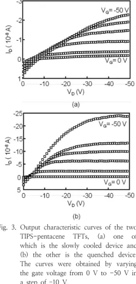
TFTs. The output characteristic curves of the two different types of devices are shown in Figs. 3(a) and 3(b). Note that output curves were observed by varying the gate voltage from 0 V to -50 V in -10 V increments. For each case, the magnitude of the drain current at both the gate voltage and drain voltage of – 50 V was about -2.5 uA (slowly cooled case) and -25 uA (quenched case). As expected from the OM images of the TIPS-pentacene distribution, the quenched case exhibited higher current due to the radially aligned TIPS-pentacene molecules which are in
Fig. 3. Output characteristic curves of the two TIPS-pentacene TFTs, (a) one of which is the slowly cooled device and (b) the other is the quenched device.
The curves were obtained by varying the gate voltage from 0 V to -50 V in a step of –10 V.
parallel with the direction of the current flow from the source electrode to the drain electrode. Interestingly, the leakage current, which is an undesirable current for TFT operation, was significantly reduced by the quenching approach. Note that the large positive drain current implies the leakage current in the Fig. 3. This might be attributed to the differently distributed TIPS-pentacene film itself. Although a study on the leakage current reduction in relation to the molecular distribution is attractive, the main aim of this study was to determine the effect of the cooling-off condition on the molecular distribution. More studies remain to be carried out in order to provide a more complete picture to understand how the electrical characteristics including the leakage current are influenced by the molecular distribution in a solution-processed organic semiconductor.
Figure 4 shows the current-voltage transfer characteristic curves. Figs. 4(a) and 4(b) represent the transfer curves for the slowly cooled case and quenched case, respectively.
From the curves, the field-effect mobility of each TIPS-pentacene TFT can be determined.
The mobility in the saturation region is theoretically given by [20]
)
2( 2
T G
D i
sat