반도체디스플레이기술학회지 제17권 제4호(2018년 12월)
Journal of the Semiconductor & Display Technology, Vol. 17, No. 4. December 2018.
66
스퍼터링 방법으로 증착한 SiO 2 와 V 2 O 5 박막의 전류특성과 계면분석
이향강
*
· 오 데레사*†
*†
청주대학교 반도체공학과Interface Characteristics and Electrical Properties of SiO 2 and V 2 O 5 Thin Films Deposited by the Sputtering
Xiangjiang Li * and Teresa Oh *†
*†
Division of Semiconductor, Choenju UniversityABSTRACT
This study was researched the electrical properties of semiconductor devices such as ITO, SiO
2
, V2
O5
thin films. The films of ITO, SiO2
, V2
O5
were deposited by the rf magnetron sputtering system with mixed gases of oxygen and argon to generate the plasma. All samples were cleaned before deposition and prepared the metal electrodes to research the current-voltage properties. The electrical characteristics of semiconductors depends on the interface’s properties at the junction. There are two kinds of junctions such as ohmic and schottky contacts in the semiconductors. In this study, the ITO thin film was shown the ohmic contact properties as the linear current-voltage curves, and the electrical characteristics of SiO2
and V2
O5
films were shown the non-linear current-voltage curves as the schottky contacts. It was confirmed that the electronic system with schottky contacts enhanced the electronic flow owing to the increment of efficiency and increased the conductivity. The schottky contact was only defined special characteristics at the semiconductor and the interface depletion layer at the junction made the schottky contact which has the effect of leakage current cutoff. Consequently the semiconductor device with shottky contact increased the electronic current flow, in spite of depletion of carriers.Key Words : ITO, SiO 2
, V2
O5,
Schottky contact, Capacitance, Junction, Depletion layer1. 서 론
1
반도체는 크기가 점점 작아지는 기술로 발전하였으며, um사이즈의 nm 사이즈로 작아지면서 기존의 반도체 소 자에서 문제가 되지 않았던 상호간접의 문제가 심각하게 나타나게 되었다. 유전체의 특성상 반도체는 벌크형에서 박막형태로 크기가 감소하면서 고주파수대에서 동작할 수 있는 작은 사이크의 회로설계가 가능하며, 상대적으로 고감도의 회로설계에 유리한 장점들을 가질 수 있게 되
† E-mail: [email protected]
었다[1-5]. 그러나 작은 사이즈는 누설전류가 발생하고 전 송선로 사이의 신호간섭으로 노이즈가 발생하여 성능이 떨어지는 단점도 동시에 나타나게 되었다. 이러한 문제점 들은 반도체 물질 중에서도 절연체의 절연 특징에 따라 서 예방이 될 수 있다. 따라서 박막의 절연물질에 대한 연구가 많이 이루어져 왔으며, 절연물질의 특성이 반도체 박막의 계면특성을 이용하여 전기적인 특성을 개선시키 려는 연구가 이루어지고 있다[6-9]. 반도체 계면특성에는 전기적인 특성이 선형적인 오믹특성과 비선형적인 쇼키 특성이 있으며, 각각의 특성이 물질마다 다르게 나타나고 플라즈마 형성에 따라서 다른 경향이 나타나고 박막의
스퍼터링 방법으로 증착한 SiO
2
와 V2
O5
박막의 전류특성과 계면분석Journal of KSDT Vol. 17, No. 4, 2018 67
크기에 따라서도 다르게 나타나고 있는 연구결과들이 많 이 보고되고 있다[10].
본 연구에서는 반도체 박막의 계면특성을 분석하기 위 해서 ITO, SiO
2
, SiO2
/ITO, V2
O5
/SiO2
,박막들을 증착하고 전기적 인 특성을 비교하여 반도체소자에서 오믹접합과 쇼키접합 의 차이점과 그에 따른 전기적인 효과에 대하여 알아보았다.2. 실험 방법
반도체 박막은 일반적인 클리닝 과정을 마치고 2 inch의 ITO, SiO2 타겟을 사용하여 rf 마그네트론 스퍼터링 방법 을 이용하여 증착하였으며, 기판은 유리를 사용하고 반응 가스로는 Ar 가스와 산소가스를 이용하였다. 증착한 박막 은 반도체계 계면에서 전자와 홀쌍의 재결합 반응이 잘 일어나도록 열처리를 실시하였다. 반도체계면특성 분석 으로 ITO, SiO2, SiO2/ITO 박막의 전기적인 측정을 위하여 Al 전극을 진공 증착하였으며, 반도체 파라미터분석기를 이용하여 I-V를 측정하였다. 반도체 물질을 이용한 각각 의 박막들의 계면특성을 분석하여 쇼키접합에 의한 절연 특성 효과에 대하여 알아보았다.
3. 실험 결과 및 고찰
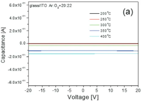
반도체 박막용 전극물질로 ITO 박막을 증착하여 열처 리를 하였다. Fig. 1(a)과 Fig. 1(b)는 ITO 박막을 200도, 250도, 300도, 350도와 400도에서 열처리를 하여 측정한 커패시턴 스와 전류-전압특성을 보여준다. ITO박막은 열처리 온도 가 달라지더라도 커패시턴스의 변화가 나타나지는 않으 며, 전류의 값은 열처리 온도가 증가할수록 증가하는 것 을 보여준다. 전류의 특성은 선형적인 특성으로 전형적인 오믹접합 특성인 것을 알 수 있다. 이러한 전도체특성은 ITO가 반도체 물질이 아니라 투명 전도체 물질이라는 것 을 알 수 있게 한다.
Fig. 2는 SiO
2
박막의 전기적인 특성을 나타낸다. Fig. 2(a) 의 커패시턴스결과는 전압이 증가함에 따라서 SiO2
박막 의 커패시턴스는 증가하고 있다. 이러한 특성은 SiO2
박막 이 n형 반도체 케리어를 갖는 특성인 것을 알 수 있으며, Fig. 2(b)의 SiO2
박막의 전기적인 특성이 비선형적인 것으 로부터 쇼키접합을 갖는 것을 알 수 있다.비선형적인 쇼키접합은 반도체계면에서 공핍층이 형성 되었다는 것을 알 수 있으며, 이러한 비선형적인 특성이 커패시턴스의 용량성을 증가한다는 것을 알 수 있다. ITO 박막은 투명전극으로써 전형적인 금속성 특징으로 오믹접 합을 가지며, SiO
2
박막은 반도체소자의 전형적인 절연물질 로써 쇼키접합 특성이 나타나고 있는 것을 확인할 수 있다.Fig. 1(a). Capacitance of ITO with various annealing
temperatures.Fig. 1(b). Electrical properties of ITO with various annealing
temperatures.Fig. 2(a). Capacitance of SiO 2
prepared on glass.Fig. 2(b). Electrical properties of SiO 2
prepared on glass.이향강 · 오 데레사
반도체디스플레이기술학회지 제17권 제4호, 2018 68
Fig. 3은 SiO
2
/ITO 박막을 증착학고 계면접합특성을 분석 하기 위해서 전기적인 특성을 측정하였다. Fig. 3(a)는 박막 증착 후 150도에서 열처리를 실시한 SiO2
/ITO 박막의 커패 시턴스는 n형 반도체 케리어를 갖는 것으로 나타나지만 커패시턴스 값이 ~10-13
F으로 상당히 낮은 값을 갖는 특징 이 있다. Fig.3(b)는 SiO2
/ITO 박막의 전류-전압특성곡선으로 써 비선형적으로 쇼키접합특성을 나타낸다. Fig. 2(b)에서 SiO2
박막의 전류값이 상당히 낮고 절연체로서 적합한 특 성으로 전도성이 낮은 쇼키접합특성을 갖는다. 그러나 그 림 Fig. 3(b)에서 전류는 비선형적인 쇼키접합특성을 가지 면서도 높은 값을 보여준다. SiO2
/ITO 박막의 증착으로 계 면에서 공핍층 효과가 더욱 우수한 쇼키접합을 형성하도 록 유도한다는 것을 알 수 있다.Fig. 3(a). Capacitance of SiO 2
prepared on ITO/glass.Fig. 3(b). Electrical properties SiO 2
prepared on ITO/glass.단일 방향을 갖는 비선형 다이오드 특성임을 알 수 있다.
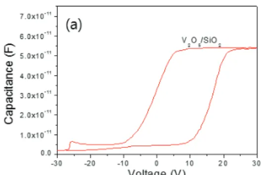
Fig. 4는 V
2
O5
/SiO2
박막을 증착하고 열처리 후전기적인 특성을 조사하면서 Fig. 2와 비교하였다. Fig. 4(a)는 V2
O5
/SiO2
박막의 n 타입 반도체 케리어를 갖는 커패시턴스의 특성 을 보여주고 있다.
Fig. 4(a). Capacitance of V 2
O5
/SiO2
thin film.Fig. 4(b). Electrical properties Capacitance of V 2
O5
/SiO2
thin film.
Fig. 4(a)의 커패시턴스는 Fig. 2(b)보다 더 안정적인 특징 을 보여준다. Fig. 4(b)에서 전류-전압특성은 Fig. 2(b)와 비교 하면 절연특성이 우수한 SiO
2
박막 위에서 V2
O5
박막의 전 류가 더 잘 통하는 높은 전도성을 가지며, 전압이 증가할 수록 Fig. 4(b)에서 더 많은 전류가 흐르고 있는 것을 알 수 있다.반도체박막은 접합계면에서 쇼키접합과 오믹접합을 형성하며, 절연박막은 쇼키접합이 유리하고 전도성박막 은 오믹접합이 유리하다. 쇼키접합은 전위장벽에 의해서 전류가 흐르는 것을 보류하면서 전도성박막의 전도성을 증가시켜주는 역할을 한다는 것을 알 수 있다. 전도성 ITO 박막은 열처리를 하더라도 오믹접합 특성만을 나타 내었으며 투명전극으로 적합한 전도성을 나타내 것을 확 인하였다. 오믹접합과 쇼키접합은 반도체 공정에서 중요 한 역할을 하면서 반도체의 전도성을 우수하게 만드는 기능을 가지며, 물질에 따라서도 공정방법에 따라서 계면 에서의 접합특성을 달라지며, 또한 반도체의 전기적인 특 성이 달라지기 때문에 반도체 소자에서 누설전류에 대한 단점을 보완할 수 있는 방법으로 계면에서 쇼키접합과 오믹접합의 형성을 이용하는 방법이 해결방법임을 알 수
스퍼터링 방법으로 증착한 SiO
2
와 V2
O5
박막의 전류특성과 계면분석Journal of KSDT Vol. 17, No. 4, 2018 69
있게 한다. 일반적으로 쇼키접합과 오믹접합은 반도체물 질 소재에 따라서 달랴졌으나 nm 급 반도체 소자에서 쇼 키접합은 반도체 계면구조적으로 계면에서 전하 혹은 케 리어들은 공핍하게 해서 만들어질 수도 있다.
4. 결 론
반도체소자의 접합특성을 알아보았다. ITO, SiO
2
, SiO2
/ ITO, V2
O5
박막들을 증착하여 준비하여 전기적인 특성으로부터 계면특성을 살펴보았다. 전도성을 갖는 ITO 박막은 오믹특 성을 나타냈으며, SiO2
와 V2
O5
박막들은 접합계면에[서 반 도체특성을 나타내는 쇼키특성을 확인하였다. ITO는 투명 전극물질로 널리 사용되고 있으며, 오믹접합에 의해서 모 든 전압에 대하여 선형적인 특징이 나타난다는 것을 확인 하였다. SiO2
와 V2
O5
박막들은 반도체소자에 많이 쓰여지는 반도체 물질로서 기본적으로 쇼키접합 특성이 나타나는 것을 필요로 하고 있으며, 쇼키접합에 의해서 누설전류가 차단되는 효과에 의해서 전압이 증가함에 따라 전도성이 높아지는 특성이 있는 것을 확인하였다.감사의 글
This work (2016013153) was supported by Mid-career Researcher Program through NRF(National Research Foundation) grant funded by the MEST(Ministry of Education, Science and Technology).
참고문헌
1. Xiongwen Zhang “Thermal Analysis of a Cylindrical Lithi-um-ion Battery,” Journal of Electrochemical Acta, 56, pp. 1246-1255, 2011.
2. Yuta Miura, Takashi Nishida, Masahiro Echizen, Yasuaki Ishikawa, Kiyoshi Uchiyama, and Yukiharu Uraoka, “Low-Operating-Voltage Solution-Processed InZnO Thin-Film Transistors Using High-k SrTa
2
O6
Li Lu1,” Japanese Journal of Applied Physics, Vol. 51, pp.03CB05, 2012.
3. Tae Eun Park, Dong Chan Kim, Bo Hyun Kong and Hyung Koun Cho, “Structural and potical properties of ZnO thin films grown by RF magnetron sputtering on Si
substrates,” Journal of the Korean Physical Society, Vol.
45, pp. S697-S700, 2004.
4. Teresa. Oh, “Analysis of Electrical Characteristics of Oxide Semiconductor of ZnO, SnO
2
and ZTO,” KoreanJournal of Materials Research, Vol. 25, No. 7, pp. 347-
351, 2015.5. Teresa. Oh, “Tunneling Condition at High Schottky Barrier and Ambipolar Transfer Characteristics in Zinc Oxide Semiconductor Thin Film Transistor,” MRB, Vol.
77, pp. 1-7, 2016.
6. Kyonghwan Oh and Oh-Kyong Kwon, “Threshold- Voltage-Shift Compensation and Suppression Method Using Hydrogenated Amorphous Silicon Thin-Film Transistors for Large Active Matrix Organic Light- Emitting Diode Displays,” Japanese Journal of Applied
Physics, Vol. 51, pp. 03CD01, 2012.
7. T. Oh and C. H. Kim “Study on Characteristic Properties of Annealed SiOC Film Prepared by Inductively Coupled Plasma Chemical Vapor Deposition,” IEEE Trans.
Plasma Science, Vol. 38, pp. 1598-1602, 2010.
8. John Robertson, Robert M. Wallace, “High-K materials and metal gates for CMOS applications,” Materials
Science and Engineering R, Vol. 88, pp. 1-41. 2015.
9. Narendra Kumar, Satyendra Kumar, Jitendra Kumar and Siddhartha Pandaa, “Investigation of Mechanisms Involved in the Enhanced Label Free Detection of Prostate Cancer Biomarkers Using Field Effect Devices,”
Journal of The Electrochemical Society, Vol. 164, No. 9,
pp. B409-B416, 2017.10. T. Oh and C. K. CHoi “Comparison between SiOC thin film fabricated by using plasma enhance chemical vapor deposition and SiO2 thin film by using fourier transform infrared spectroscopy,” Journal of the Korean Physical
Society, Vol. 56, pp. 1150-1155, 2010.
11. Young Seok Lee, Jang Jae Lee, Si Jun Kim and Shin Jae You, “Research on the relative comtribution of two electron groups of Ar plasma with non-thermal equilibrium electron distribution,” Journal of the
Semiconductor & Display Technology, Vol. 17, No. 11,
pp. 76-83, 2018.접수일: 2018년 12월 10일, 심사일: 2018년 12월 13일, 게재확정일: 2018년 12월 18일