http://dx.doi.org/10.5369/JSST.2017.26.2.122 pISSN 1225-5475/eISSN 2093-7563
큰 결정 크기를 가지는 단일층 그래핀 성장을 위한 구리 호일의 전해연마 공정 최적화
김재억 · 박홍식+
Optimized Electroplishing Process of Copper Foil Surface for Growth of Single Layer Graphene with Large Grain Size
Jaeeuk Kim and Hongsik Park+
Abstract
Graphene grown on copper-foil substrates by chemical vapor deposition (CVD) has been attracting interest for sensor applications due to an extraordinary high surface-to-volume ratio and capability of large-scale device fabrication. However, CVD graphene has a polycrystalline structure and a high density of grain boundaries degrading its electrical properties. Recently, processes such as elec- tropolishing for flattening copper substrate has been applied before growth in order to increase the grain size of graphene. In this study, we systemically analyzed the effects of the process condition of electropolishing copper foil on the quality of CVD graphene. We observed that electropolishing process can reduce surface roughness of copper foil, increase the grain size of CVD graphene, and min- imize the density of double-layered graphene regions. However, excessive process time can rather increase the copper foil surface rough- ness and degrade the quality of CVD graphene layers. This work shows that an optimized electropolishing process on copper substrates is critical to obtain high-quality and uniformity CVD graphene which is essential for practical sensor applications.
Keywords: graphene, electropolishing, surface roughness, grain boundary
1. 서 론
그래핀은 탄소원자들이 육각형 구조로 평면을 따라 배열된 형 태의 이차원 물질로, 우수한 전기적, 기계적 특성으로 인해 다 양한 소자의 재료로 적용되고 있다[1]. 특히, 그래핀은 높은 표 면 대 체적 비율을 가짐으로써 센서 소자의 재료로 활용하는 데 에도 큰 장점이 있다[1-7].
그래핀을 센서에 활용하는 데에는 전기적 특성이 균일한 단 일층 그래핀을 대면적으로 합성하는 것이 필수적이다. 대표적인 그래핀 제작법으로는 흑연에서 그래핀 층과 층 사이의 약한 상 호작용을 기계적인 힘으로 떼어내는 기계적 박리법[8], 산화된 흑연을 파쇄한 후 수용액 상에 분산된 산화 그래핀을 환원제를 이용하여 그래핀으로 되돌리는 화학적 박리법[9], 메탄 등의 탄
소를 포함하고 있는 전구체와 수소가스가 반응하여 생성된 탄 소 원자들이 니켈이나 구리와 같은 전이금속 촉매에 용해되거 나 흡착되고, 이후 냉각 과정에서 촉매 층에 포함된 탄소가 표 면에서 그래핀을 결정구조를 형성하는 화학기상증착법(chemical vapor deposition, CVD)[10], 실리콘카바이드(SiC)기판을 고온에 서 열처리 하여 결정 내에 포함되어 있던 탄소가 표면으로 분 리되어 그래핀을 형성하는 에피택셜 합성법[11]이 있다. 위 방 법들 중 화학기상증착법은 낮은 비용으로 대면적의 그래핀을 합 성할 수 있고 합성된 그래핀을 다른 기판에 전사하는 것이 용 이하여 소자제작에 가장 많이 사용되고 있는 기술이다. 하지 만, 화학기상증착법으로 합성된 그래핀은 합성 과정에서 다결정 구조를 형성하므로 결정 간 경계(grain boundary)에서 전기적 특 성이 저하된다는 단점이 있다[12-14]. 이를 개선하기 위해 최근 에 전해연마[15] 또는 화학기계연마 (chemical mechanical polishing, CMP)[16] 처리를 통해 표면이 평탄해진 구리 호일 위에 그래핀을 합성하여 그래핀의 평균적인 결정 크기(grain size) 를 키우는 연구들이 진행되고 있다. 본 논문에서는 전해연마 공 정조건이 합성된 그래핀의 특성에 중요한 영향을 미친다는 것 을 결과로 제시한다. 전해연마 공정시간이 구리 호일의 표면 거 칠기에 미치는 영향과 구리 호일의 표면 거칠기의 제어가 화학 기상증착 법으로 합성된 그래핀의 grain size와 다층 그래핀의 형성에 미치는 영향을 체계적으로 분석하였다. 전해연마 공정시
경북대학교 전자공학부(School of Electronics Engineering, KyungpookNational University)
80 Daehakro, Bukgu, Daegu, 41566, Korea
+Corresponding author: [email protected]
(Received: Mar. 6, 2017, Revised: Mar. 24, 2017, Accepted: Mar. 25, 2017)
This is an Open Access article distributed under the terms of the Creative Commons Attribution Non-Commercial License(http://creativecommons.org/
licenses/bync/3.0) which permits unrestricted non-commercial use, distribution, and reproduction in any medium, provided the original work is properly cited.
간을 변화시키며 그래핀 합성 실험을 수행한 결과, 구리 호일의 표면 거칠기를 최소화하는 특정 시간이 존재하였고, 이 최적 조 건에서 합성된 그래핀은 가장 큰 grain size와 가장 낮은 밀도의 다층 그래핀 영역을 가지는 것으로 확인되었다.
2. 실험 방법
2.1 구리 호일 기판 전해연마 공정
전해연마는 금속 표면의 산화·환원 반응을 이용한 공정이다.
산성 전해질 용액에 두 금속 전극(anode 와 cathode)을 담근 후 DC 전압을 걸어주면 anode극의 표면에 위치한 금속 원자는 전 자를 잃고 이온화(산화)되고, cathode 극의 표면에서는 전해질 내부에 존재하는 수소 이온이 전자를 받고 환원되어 수소 가스 가 발생한다. 이 때, anode 극에서 표면이 뾰족한 부분이 평탄 한 부분에 비해 표면적이 넓기 때문에 산화반응이 더 활발하게 일어나고 이로 인해 anode 극의 표면이 전체적으로 평탄해지는 결과를 가져온다. Fig. 1(a)는 전해연마 공정에 따른 금속 표면 의 profile을 개략적으로 나타낸 것이다. 이미지에서 볼 수 있듯 이, 전해연마 공정은 구리 호일 표면의 거친 부분을 감소시키는 효과가 있다. Fig. 1(b)는 본 논문에서 구리 호일의 전해연마 처 리를 위해 사용한homemade electrolytic cell의 개략도이다. 전 해질로는 85% 농도의 인산(H
3PO
4) 수용액을 사용하였으며, cathode와 anode로는 동일한 크기(2.2 cm × 10 cm)의 두 구리 호일(25 µm 두께, Alfa Aesar사, 46365)조각을 각각 사용했다.
DC 전압은 0.2~1.2 V까지 0.1 V 간격으로 10초마다 상승시켰으
며 이후 1.2 V를 유지하였다. 전해연마 공정시간은 15~40분으 로 바꿔가며 실험하였고, 그 후 초순수(ultrapure water, UPW) 를 이용한 rinsing 공정 및 N
2drying 공정을 진행하였다. Fig.
1(c), (d)는 전해연마 공정 전, 후의 구리 호일 표면을 공초점 현 미경(confocal microscope, CM)으로 관찰한 이미지이다. Fig. 1(c) 와 (d)를 비교해 보면, 구리 호일 표면의 굴곡들이 전해연마 공 정 후 감소하는 것을 확인할 수 있다.
2.2 그래핀 합성 및 UV/ozone 산화 처리
Fig. 2(a) 는 본 연구에서 그래핀을 합성하는데 사용한 열화학 기상증착장비(thermal chemical vapor deposition, TCVD)의 개 략도이다. 전해연마 공정을 진행하지 않은 구리 호일 샘플과 전 해연마 공정을 15, 20, 30, 40분 동안 진행한 샘플들을 챔버(chamber) 의 내부에 위치시킨 후 1050
oC 에서 그래핀을 합성하였다. 그래 핀은 2 sccm의 CH
4, 100 sccm의 H
2, 그리고 570 sccm의 Ar 가 스를 흘려주는 조건에서 합성되었으며, 가스들의 유량은 질량유 량계(mass flow controller, MFC)를 통해 제어하였다.
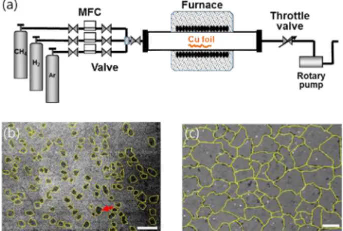
Fig. 2(b)는 TCVD로 구리 호일 위에 합성한 그래핀의 주사 전자현미경 (scanning electron microscope, SEM) 이미지이다.
붉은 화살표가 가리키는 부분처럼 주변보다 어두운 영역이 다 수 분포해 있는데, 이러한 영역들은 다층 그래핀이 부분적으로 형성되었음을 의미한다[10]. 구리 호일 위에 합성된 그래핀은 별 도의 표면 처리 없이는 grain boundary를 관찰하기 어렵지만, 이 를 습한 환경에서 UV/ozone 산화 처리하면 그래핀 grain boundary 아래의 구리 영역만 선택적으로 산화가 가능하며 이를 이용하 여 그래핀의 grain boundary를 광학현미경(optical microscopy) 또는 SEM으로 관찰이 가능하다[17]. 본 실험에서는 그래핀의 grain boundary를 SEM으로 관찰하기 위해 Novascan 사의 UV/
ozone cleaner 장비를 사용하여 30 분간 UV/ozone 산화 공정을 Fig. 1. Schematic of (a) surface flattening of copper foil substrate
electropolishing process and (b) homemade electrolytic cell used for the electropolishing process. Confocal microscope images of copper foils (c) before surface treatment and (d) after electropolishing process. Scale bars: 20 µm.
Fig. 2. (a) Schematic diagram of TCVD system for graphene growth.
SEM images of (b) as-grown graphene layer and (c) visu-
alization of grain boundaries of graphene by UV/ozone oxi-
dation process. Scale bars: 10 µm.
진행하였다. Fig. 2(c)는 구리 호일 위에 합성된 그래핀을 UV/
ozone 산화 처리 후 SEM으로 관찰한 이미지이다. 산화 처리를 통해 시각화 된 그래핀의 grain boundary를 보다 명확하게 구분 할 수 있도록 ImageJ 소프트웨어를 이용하여 노란 실선으로 표 시하였다.
3. 결과 및 고찰
3.1 전해연마 공정이 구리 호일 표면 거칠기에 미치는 영향
전해연마 공정시간이 구리 호일의 표면 거칠기에 미치는 영 향을 Fig. 3에 나타냈다. Fig. 3(a)는 전해연마 처리를 하지 않 은 구리 호일, Fig. 3(b)-(e)는 각각 15, 20, 30, 40분 동안 전해 연마 공정을 진행한 구리 호일의 표면을 CM으로 관찰한 이미 지이다. Fig. 3(a)에서 볼 수 있듯이, 전해연마 처리 공정을 수 행하지 않은 구리 호일의 표면에는 많은 굴곡들이 존재하고 이 런 굴곡들은 표면을 거칠게 하는 주요 원인이다. 전해연마 공정 은 이러한 구리 호일의 굴곡들을 식각하여 표면의 거칠기를 낮 추는 효과가 있지만[Fig. 3(b), (c)], 과도하게 공정을 진행할 경 우 표면이 움푹 패여 (crater형성) 오히려 거칠기가 상승한다[Fig.
3(d), (e)]. Fig. 3(f)-(j)는 전해연마 공정시간에 따른 구리 호일
표면의 line profile 측정 결과를 나타낸 것이다. 앞서 설명한 것 과 같이 전해연마 공정을 20분동안 진행했을 때의 표면이 가장 매끄러웠으며, 더 긴 시간동안 전해연마 공정이 진행된 구리 호 일들은 상대적으로 표면 거칠기가 상승하였다. Fig. 3(k)는 구리 호일 표면 거칠기와 전해연마 공정시간의 관계를 공정조건에 따 라 각각 4장의 CM 이미지를 측정한 결과를 이용하여 나타낸 그래프이다. 전해연마 공정을 20분 동안 진행했던 샘플의 표면 거칠기 root mean square값(R
sq) 은 0.11 µm로, 전해연마 공정을 수행하지 않은 샘플(R
sq= 0.33 µm), 15 분 (R
sq= 0.24 µm), 30분 (R
sq= 0.25 µm), 40분(R
sq= 0.32 µm) 동안 전해연마 공정을 진 행한 샘플들에 비해 값이 가장 낮았다. 위의 결과는 전해연마 공정으로 구리 호일의 표면 거칠기를 낮추는 데 있어서 최적의 공정시간이 존재하며, 이보다 더 과도한 전해연마 공정을 진행 할 경우, 구리 호일의 표면이 더 거칠어진다는 것을 보여준다.
3.2 구리 호일 표면 거칠기와 그래핀 grain size의 상관관계
화학기상증착법으로 합성된 그래핀은 다결정 구조를 형성하 므로 grain boundary에서 전기적 특성이 저하된다. 이를 최소화 하기 위해서는 합성된 그래핀의 평균적인 grain size를 키움으 로써 grain boundary의 밀도를 줄이는 것이 필수적이다. 그래핀 의 grain size는 초기 합성 단계에 생성된 그래핀 nucleation seeds Fig. 3. Effect of electropolishing process on the surface roughness of copper foils. Confocal microscopy images of copper foils with different process time [(a) no treatment, (b) for 15-minutes, (c) for 20-minutes, (d) for 30-minutes, and (e) for 40-minutes]. Scale bars: 20 µm.
Line profiles of copper foils with different process time [(f) no treatment, (g) for 15-minutes, (h) for 20-minutes, (i) for 30-minutes, and
(j) for 40-minutes] (k) Plot of RMS surface roughness of the electropolished copper foils from 4 confocal microscope images for each
sample indicating that foil copper with 20-minutes electropolishing process has the minimized surface roughness.
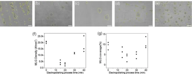
의 밀도에 크게 영향을 받는데, 연마공정을 통해 구리 호일의 표면 거칠기를 감소시키면 그래핀 nucleation seeds의 밀도를 낮 출 수 있다[15,16]. 구리 호일의 전해연마 공정시간과 합성된 그 래핀의 grain size의 상관관계를 Fig. 4에 나타내었다. Fig. 4(a) 는 전해연마 처리를 하지 않은 구리 호일, Fig. 4(b)-(e)는 각각 15, 20, 30, 40 분 동안 전해연마 공정을 진행한 구리 호일 위에 합성된 그래핀을 UV/ozone 산화 처리 한 후 SEM으로 관찰한 이미지이다. 산화 처리를 통해 시각화 된 그래핀의 grain boundary 는 ImageJ소프트웨어를 이용하여 노란 실선으로 표시하였다.
Fig. 3(a)-(e) 의 결과와 비교하여, 구리 호일의 표면 거칠기 값이 낮을수록 그 위에 합성된 그래핀의 grain size가 커지는 것을 알 수 있다. Fig. 4(f)는 각각 다른 시간동안 전해연마 공정을 시행 한 구리 호일 위에 합성된 그래핀의 평균 grain size를 전해연마
공정시간에 따라 0~40 분까지의 순서로 각각 222, 81, 38, 60, 103 개의 측정 결과로부터 얻은 데이터를 분석한 그래프이다. 전 해연마 공정을 20분 동안 진행한 구리 호일 위에 합성된 그래 핀의 평균 grain size는 11.2 µm로, 공정을 수행하지 않은 샘플 (4.34 µm), 15 분 (8.34 µm), 30분(8.89 µm), 40분(6.01 µm) 동안 공정을 진행한 구리 호일을 이용하여 합성된 그래핀들에 비해 평균 grain size가 크게 나타났다. 이 결과는 전해연마 공정을 통 해 구리 호일의 표면을 최대한 평탄화 하는 것이 화학기상증착 법으로 합성된 그래핀의 grain size를 키우는 데에 중요함을 보여준다.
3.3 구리 호일 표면 거칠기가 다층 그래핀의 형성에 미치 는 영향
그래핀의 전기적 특성에 영향을 미치는 요인으로는 grain
Fig. 4. Effect of electropolishing process on the average grain size of the graphene layers. SEM images of graphene layers grown on the copper foils polished with different process time [(a) no treatment, (b) for 15-minutes, (c) for 20-minutes, (d) for 30-minutes, and (e) for 40- minutes]. The grain boundaries in these images were oxidized by UV/ozone treatment and highlighted with yellow lines. Scale bars:
5 µm. (f) Plot of average grain sizes of the graphene layers indicating that the graphene layer on the copper substrate with minimized roughness has the largest grain size.
Fig. 5. Effect of copper foil electropolishing on multilayer graphene (MLG) formation. SEM images of graphene layers grown on the copper foils polished with different process time [(a) no treatment, (b) for 15-minutes, (c) for 20-minutes, (d) for 30-minutes, and (e) for 40- minutes] . Scale bars: 5 µm. Plots of (f) MLG density and (g) MLG coverage of graphene grown on the electropolished copper foils.
Graphene grown on 20-minutes electropolished copper foil show the lowest MLG density and coverage.
boundary 이외에도 그래핀의 층 수가 있다. 다층 그래핀 (multilayer graphene, MLG) 은 단일층 그래핀 (single layer graphene, SLG) 에 비해 이동도가 떨어지는 경향이 있어서 높은 이동도를 가지 는 그래핀을 얻기 위해서는 MLG의 형성을 억제할 필요가 있 다[18]. MLG의 형성은 구리 호일이 SLG로 덮인 뒤에 성장하 기 시작하는데, SLG 합성 초기에 생성된 nucleation seeds를 중 심으로 MLG가 형성되기 시작한다[19]. Fig. 5(a)는 전해연마 처 리를 하지 않은 구리 호일, Fig.5(b)-(e)는 각각 15, 20, 30, 40분 동안 전해연마 공정을 진행한 구리 호일 위에 합성된 그래핀을 SEM 으로 관찰한 이미지이다. MLG 영역은 ImageJ소프트웨어 를 이용하여 노란 실선으로 표시하였다. Fig. 3(a)-(e)의 결과와 비교하여, 구리 호일의 표면 거칠기 값이 클수록 MLG가 많이 형성되는 것을 알 수 있다. Fig. 5(f)와 (g)는 각각 MLG의 밀도 와 전체 면적 중 MLG가 차지하는 면적의 비율을 나타낸 그래 프이다. 각 그래프들을 Fig. 3(k)와 비교해 보면, 구리 호일의 표 면 거칠기 값이 낮을수록 MLG의 형성이 억제되는 것을 확인 할 수 있다.
4. 결 론
본 연구에서는 그래핀의 전기적 특성 향상을 위한 최적의 구 리 호일 전해연마 공정조건을 발견하였다. 전해연마 공정은 구 리 호일의 표면 거칠기를 낮추는데 효과적인 공정으로, 이를 이 용하여 그래핀을 합성할 경우 쉽게 평균 grain size를 키우고, MLG의 형성을 억제할 수 있다. 하지만, 과도하게 전해연마 공 정을 진행할 경우, 오히려 구리 호일 표면에 crater들을 다수 형 성하여 표면이 더욱 거칠어지고, 그 결과 합성된 그래핀의 평균 grain size 가 작아지는 경향을 보였다. 본 연구 결과는 화학기상 증착법으로 합성된 그래핀의 전기적 특성을 향상시킴으로써, 그 래핀이 다양한 센서에 활용되는 데에 기여할 수 있을 것으로 기대된다.
감사의 글
본 연구는 산업통상자원부 및 한국산업기술평가관리원의 센 서산업고도화를 위한 첨단센서육성사업(10054570)과 교육부 재 원의 한국 연구재단(NRF)기초연구사업 (2015R1D1A1A01060861) 의 지원을 받아 수행되었음.
REFERENCES