pISSN 1229-3008 eISSN 2287-6251
Progress in Superconductivity and Cryogenics
Vol.17, No.2, (2015), pp1~17 http://dx.doi.org/10.9714/psac.2015.17.2.001
```
1. INTRODUCTION
The discovery of superconductivity in MgB2 with a transition temperature (Tc) of 39 K [1, 2] is the greatest advantage over conventional metallic superconductors, such as NbTi (Tc = 9 K) and Nb3Sn (Tc= 18 K). In addition, long coherence length [3], high critical current densities [4], and strongly linked nature of the intergrains [5] with a high charge carrier density [6] portrays MgB2 as a potential material for applications, such as superconducting magnets, electronic devices, and coated conductor wires for power applications [7]. MgB2 devices and circuits can be operated above 20 K. A 20 K cooler requires much less input power, is much lighter, and costs much less than a 4 K cooler with the same cooling power. Columbus Superconductors has fabricated the first kilometer range length MgB2 tapes up to 1.6 km in 2006 by ex situ powder-in-tube (PIT) process [8].
Hyper Tech Research, Inc., (Hyper Tech) has used continuous tube filling and forming (CTFF) process to fabricate the multifilament MgB2 wire constructed with 18 monofilaments (Nb barrier, Cu sheath) and one center copper filament restacked in Monel [9]. The cryogenic free magnet of 0.6 T, solenoid and fault current limiters prototypes were also produced from MgB2 wires. Recently, Yamamoto et al. demonstrated that 40-K-class metallic magnesium diboride (MgB2) makes an excellent permanent bulk magnet, maintaining 3 T at 20 K for 1 week with an extremely high stability (<0.1 ppm/h) [10]. Very recently, a world-record current of 20 kA at 24 K in an electrical transmission line consisting of two 20-metre long cables made of MgB2 superconductor was obtained by CERN
superconductors team [11]. All these demonstrate that MgB2 has potential practical scope and applicability i electrical and power engineering devices, such as fault current limiters, motors, and transformers, as well as magnet systems, especially in MRI.
Among all forms of MgB2, such as single crystal, bulk, thin films, wires, and tapes, MgB2 thin films show a highest Tc of 41.8 K, low resistivity (ρ300K =6.7 µΩ·cm and ρ41K = 0.24 µΩ·cm), and high critical current density, Jc(0) of >
107 A/cm2 [12]. A variety of thin film techniques have been used to grown MgB2 thin films, such as co-evaporation [13, 14], pulse laser deposition (PLD) [2, 15], sputtering [16, 17], molecular beam epitaxy (MBE) [18–20], laser-assisted chemical vapor deposition (LACVD) [21, 22], and hybrid physical-chemical vapor deposition (HPCVD) [12, 23].
Among all these techniques, HPCVD has been proved to be the most effective one for the fabrication of high-quality MgB2 films with superior superconducting properties. A very high magnetic and transport Jc(0) of 5 × 10⁷ A cm-2 at 5 K [24] and Jc(0) of 1.6 × 10⁸ A cm-2 [4], respectively for pure HPCVD films, and a record high upper critical field (Hc2) over 60 T were obtained for carbon-doped HPCVD films [25]. Such extraordinary Hc2 values for carbon-doped MgB2 films are well above from those of standard high-field Nb-based superconductor materials. In addition by using HPCVD, different kinds of MgB2 films can be produced, such as single-crystal like MgB2 thin films, MgB2 epitaxial columnar thick films, and a-axis-oriented MgB2 films. HPCVD system was also employed to fabricate MgB2 coated-conductors (CC) [26-29] with dense MgB2 phase which is not possible by powder-in-tube (PIT) process due to its low packing density problem [30]. MgB2
A review on the understanding and fabrication advancement of MgB
2thin and thick films by HPCVD
Mahipal Ranot, P. V. Duong, A. Bhardwaj, and W. N. Kang*
BK21 Physics Division and Department of Physics, Sungkyunkwan University, Suwon 440-746, Korea (Received 3 June 2015; revised or reviewed 8 June 2015; accepted 9 June 2015)
Abstract
MgB2 thin films with superior superconducting properties are very promising for superconducting magnets, electronic devices and coated conductor electric power applications. A clear understanding of flux pinning mechanism in MgB2 films could be a big aid in improving the performance of MgB2 by the enhancement of Jc. The fabrication advancement and the understanding of flux pinning mechanism of MgB2 thin and thick films fabricated by using hybrid physical-chemical vapor deposition (HPCVD) are reviewed. The distinct kind of MgB2 films, such as single-crystal like MgB2 thin films, MgB2 epitaxial columnar thick films, and a-axis-oriented MgB2 films are included for flux pinning mechanism investigation. Various attempts made by researchers to improve further the flux pinning property and Jc performance by means of doping in MgB2 thin films by using HPCVD are also summarized.
Keywords: MgB2 thin and thick films, HPCVD, flux pinning mechanism
* Corresponding author: email: [email protected]
A review on the understanding and fabrication advancement of MgB2 thin and thick films by HPCVD
CCs showed self-field Jc values of the order of 107 A/cm2 at 5 K as high as already obtained in MgB2 thin films, however, Jc decreases in response to an applied magnetic field [31, 32]. Therefore, a complete understanding of the flux pinning mechanism could be a big aid in improving the performance of MgB2 by the enhancement of Jc, which is most important parameter in practical applications for an operation with low noise and lower power loss. The epitaxial MgB2 thin films with uniform orientation of grains provide an ideal condition for investigating the vortex dynamics and flux pinning properties, in contrast to MgB2 bulk system where grains are randomly orientated. In this article, we review the progress made in the last 14 years for the fabrication, understanding of flux pinning mechanism, and for improving the performance by doping in MgB2 epitaxial thin and thick films by using HPCVD technique.
2. HPCVD TECHNIQUE
The HPCVD technique was firstly developed by Xi et al.
to generate high Mg vapor pressure, impractical for many vacuum deposition techniques, is necessary to keep the MgB2 phase thermodynamically stable at elevated temperatures [12]. Our HPCVD system [23, 33] is similar to them. For MgB2 film growth, HPCVD process uses diborane (B2H6) as the boron precursor gas, but unlike conventional CVD, which only uses gaseous sources, heated bulk magnesium pieces are used as the Mg source in the deposition process. Since the process involves chemical decomposition of precursor gas and physical evaporation of metal bulk, it is named as hybrid physical-chemical vapor deposition.
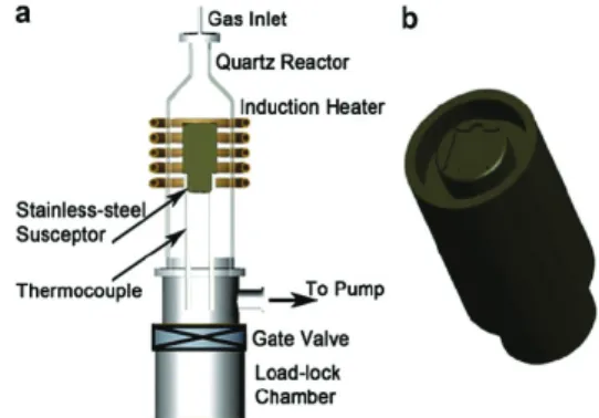
The schematic diagram of the HPCVD system is shown in Fig. 1(a). It consists of a vertical quartz tube reactor having a bell shape (inner diameter: 65 mm, height: 200 mm), gas inlet and flow control system, pressure maintenance system, temperature control system, gas exhaust and cleaning system, inductively coupled heater, and a load-lock chamber. The main process chamber is connected with the load-lock chamber on the bottom and an induction heater is attached on the outer periphery of the process chamber. A susceptor made from stainless steel is placed coaxially inside the reactor as shown in Fig. 1(b).
There is a gate-valve between the process chamber and the load-lock chamber. This valve protects the process chamber from contamination during the synthesis of MgB2
films.
For MgB2 film growth, the process chamber was purged several times with ultra high purity (99.9999%) Ar gas.
After that the susceptor along with substrate and 3 - 6 g of granular Mg chips (99.999%) (diameter: 2 - 3 mm) was installed in the reactor. The substrate and solid Mg chips sit on the same susceptor are heated up inductively at the same time to the set temperature (Ts) under the working pressure (Pw) in ambient H2. Upon attaining the set temperature, the bulk Mg pieces melts and generates a high vapor pressure in the vicinity of the substrate. Then the precursor gas B2H6
Fig. 1. (a) Schematic diagram of the HPCVD system. (b) The susceptor on which substrate is mounted on the top.
About 6.5 g of Mg can be accommodated around the substrate holder, good enough to maintain high Mg vapor pressure during deposition.
(5% in H2 gas) is introduced into the chamber and decomposes around the substrate at high temperature. The atoms from the decomposed precursor gas react with the Mg vapor, forming thin films on the substrate by the following chemical equation,
B2H6+Mg→MgB2+3H2
The deposition ends when the precursor gas is switched off.
The growth mechanism of MgB2 film followed the Volmer-Weber growth mode. In the Volmer-Weber growth mode, the smallest stable clusters nucleate on the substrate and grow in 3D to form islands. At the beginning of the growth, islands of hexagonal shaped MgB2 form on the substrate, which grow and coalesce into a continuous film at larger film thickness. When the islands coalesce, they
‘‘zip up’’ because the surface energy of the islands is larger than the free energy of the grain boundaries. The more detail on the deposition technique and mechanism can be found in [34].
3. MgB2 FILMS BY HPCVD 3.1. Single-crystal like MgB2 thin films
Most fundamental research on MgB2 is carried out using single crystals, requires both high-pressure and high-temperature fabrication conditions, and involves a very long growth time [35, 36]. At the moment, however, the sizes of the MgB2 single crystals are very small [35]. As a result, MgB2 thin films have been produced and employed in the study of two-gap superconductivity in MgB2. Furthermore, the high-quality MgB2 thin films are very suitable for engineering applications, such as superconducting electronic devices [37] and radio-frequency (RF) cavities [38, 39]. For example, Nb-based RF cavity technology is now very close to theoretical limits [38] and high-quality single-crystalline MgB2 thin films are considered to be the most plausible candidates [39] for meeting the still expanding requirements of accelerator research.
The single-crystal MgB2 thin films with large area were fabricated on c-plane Al2O3 substrates by using HPCVD 2
Mahipal Ranot, P. V. Duong, A. Bhardwaj, and W. N. Kang
Fig. 2. XRD scan, showing only the (000l) peaks of MgB2, with substrate peaks being marked by the solid diamond.
[24]. The fabrication of a single-crystalline film on a cheap substrate, such as Al2O3, will be more beneficial for practical applications. The excellent thermal conductivity and the optical properties of Al2O3 provide further advantages for practical applications at low temperatures.
The X-ray diffraction (XRD) results are shown in Fig. 2.
Only (000l) peaks, without any impurity or secondary phases are observed. The c-axis lattice constant determined from the (0002) peak is 3.519 Å, slightly smaller than the bulk value of 3.521 Å. The full width at half maximum (FWHM) obtained from the rocking curve for the (0002) peak [inset of Fig. 2] is as low as 0.13°, which is very close to that for a MgB2 single crystal [40] and is much narrower than that for an epitaxial MgB2 thin film grown on a (0001) SiC substrate [4], indicating that the MgB2 thin film grown on a (0001) Al2O3 substrate has a single-crystal quality.
The complete detail on fabrication and growth mechanism of the single-crystal MgB2 film on (000l) Al2O3 substrate can be found elsewhere [24].
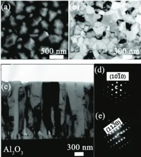
Bright-field transmission electron microscopy (TEM) images [Fig. 3(a): cross-sectional view, 3(b): planar view]
also indicate a single-crystal quality without grain boundaries. The MgB2 thin film with a thickness of 780 nm was very smooth without any grain boundaries.
Selected-area electron diffraction (SAED) patterns for the interface between MgB2 film and substrate are shown in Fig.
3(c). Very clear spots can be classified into two sets: one corresponds to the MgB2 film, the other belongs to the Al2O3 substrate. No other phase diffraction spots were observed, which consistent with the XRD results. The SAED patterns for the surface of the MgB2 film [Fig. 3(d)]
clearly reflect the hexagonal structure of the single-crystal MgB2. The planar hexagonal structure can be more directly seen in the high-resolution TEM image shown in Fig. 3(e).
All these results suggest that the MgB2 thin film is well aligned not only along the c-axis but also along the planar direction. The a-axis lattice parameter was found to be 3.088 Å, which is slightly larger than that of 3.086 Å reported for bulk MgB2 [41].
Fig. 3. (a) Low-magnification bright-field cross-sectional TEM image. Platinum was deposited for protection. (b) Low-magnification bright-field planar TEM image. (c) Cross-sectional SAED pattern near the interface region. (d) Planar SAED pattern from the top surface of the MgB2
layer. (e) High-resolution TEM image. (f) Perspective schematic illustration for the observed perfect long-range lattice-matching relation between the Al2O3 lattice (blue color) and MgB2 (red color). The a-axis of the MgB2 layer is rotated 30o with respect to that of the substrate (yellow color). A long-range order can be seen at the green-color circles.
The lattice mismatch between MgB2 and Al2O3 is as large as 23% where the a-axis lattice constant of Al2O3 is 4.758 Å. A question arises, how a single-crystal MgB2 thin film can be grown so perfectly on a (0001) Al2O3 substrate?
A clue to the solution is provided by the cross sectional SAED patterns in which the (100) direction of the MgB2
layer is aligned parallel to the (110) direction of the Al2O3
substrate. A perspective schematic illustration at the interface between MgB2 and Al2O3 is presented in Fig. 3(f), where the hexagonal Al2O3 and MgB2 lattices are depicted as blue and red colors, respectively. The a-axis of the MgB2
film is rotated 30° with respect to that of the substrate, as highlighted in yellow colors in Fig. 3(f). This 30° rotation leads to an interesting long-range lattice-matching order.
The additional points where the locations of Mg and Al coincide with each other are colored green in Fig. 3(f). The growth mechanism exhibited a perfect domain-lattice 3
A review on the understanding and fabrication advancement of MgB2 thin and thick films by HPCVD
matching ratio of 8aMg : 3aAl between the a-axis lattice constant (aMg) of MgB2 and the a-axis lattice constant (aAl) of Al2O3 for the case in which the (110) plane of MgB2 was parallel to the (100) plane of Al2O3. Indeed, 8aMg = 24.704 Å and 3aAl = 24.727 Å, showing a perfect matching relation with a mismatching ratio of less than 0.1%. As a result, we are able to successfully grow single-crystal MgB2 thin films with superior quality on (0001) Al2O3 substrates.
The onset transition temperature of single-crystal MgB2
thin film is observed to be 40 K with a very sharp transition width of 0.1 K. The resistivity at room temperature (300 K) was about 6.7 µΩ·cm, but it decreased to 0.24 µΩ·cm at 41 K. The residual resistivity ratio (RRR) is as high as 28. The single-crystal MgB2 thin films are cleaner than the reported single-crystal [42] and bulk samples [43]. The high RRR value and the very low resistivity at 41 K indicate that the MgB2 film has a very long electron mean free path owing to the low number of crystallographic defects. Very clean epitaxial MgB2 thin films on SiC substrates were also demonstrated by Xi et al. using HPCVD [12].
Pogrebnyakov et al. studied the effect of deposition rate and layer thickness on the properties of epitaxial MgB2 thin films grown by HPCVD on 4H-SiC substrates. They found that the deposition rate of MgB2 films by HPCVD is proportional to the B2H6 gas mixture flow rate, consistent with the thermodynamic prediction of the adsorption-controlled growth of MgB2. The high deposition rate leads to larger grain sizes and the film roughness increases with the film thickness. The superconducting and normal-state transport properties, however, do not depend on the deposition rate, but rather on the MgB2 film thickness. Larger film thickness results in higher Tc, lower ρ0, and higher RRR [44]. Li et al. reported a large anisotropic normal-state magnetoresistance (∆ρ/ρ0=136% for the H┴ab plane at 18T) in clean MgB2
thin films [45]. This is a direct result of the multiband nature of MgB2 and the cleanness of the HPCVD films. For a single-band free-electron system, the Hall field exactly balances the Lorentz force and therefore there is no magnetoresistance. However, if there are two or more bands of different carriers, the Hall field cannot exactly cancel the Lorentz force and there will be magnetoresistance. By fitting the normal-state magnetoresistance data, they found that both the σ and π bands of pure HPCVD films are in the clean limit. The low surface resistance for HPCVD films was reported by Jin et el. which is very useful for microwave device and THz electronic applications [46]. Ye et al. found that the HPCVD films are free from dendritic flux jumps which are frequently observed in PLD films and MgB2 bulk samples [47]. The cleanness of the HPCVD film and its low normal state resistivity is believed to be the key factors in enhancing the magnetic stability at low temperatures.
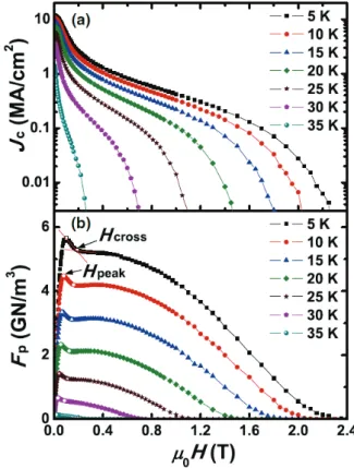
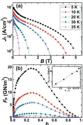
The field dependences of the critical current density (Jc) at 5 and 20 K for single crystal MgB2 thin films are shown in Fig. 4(a). The Jc was calculated from the M–H loops by Bean’s critical state model (Jc=30Δm/rV), where Δm is the height of the M–H loop, r is the radius corresponding to the total area of the film surface and V is the sample volume.
The self-field Jc was as high as 5 × 10⁷ A cm-2 at 5 K and 3
× 107 A cm-2 at 20 K, which is very close to the depairing current density and shows the ultimate current-carrying capability of MgB2. Zhuang et al. [4] report the observation of a very high Jc(0) of 1.6 × 10⁸ A cm-2 by the transport measurement in a clean-limit MgB2 film grown by HPCVD, the highest self-field Jc observed so far in MgB2. These high Jc values in HPCVD films suggest that MgB2 has a great potential in practical applications. However, the Jc
rapidly decreased with an increasing applied field owing to the lack of pinning centers in clean films, as observed for single crystals. Therefore, the enhancement in Jc is the most important issue in practical applications of MgB2
superconductor. Flux pinning, which leads to a frozen vortex state at current densities below the Jc, protects superconductors from power dissipation. A complete understanding of the flux pinning mechanism could be a big aid in studies related to this issue. We considered that our single-crystal MgB2 thin films are the idea system to investigate fundamental superconducting properties, such as flux pinning and vortex dynamics. The detailed analyses and explanation on flux pinning mechanism in single-crystalline MgB2 thin films can be found in Ref.
[48].
Fig. 4. (a) Magnetic field dependences of the critical current density (Jc) and (b) the flux pinning force density (Fp) at various temperatures for single-crystalline MgB2
thin films. Unusual peaks near zero fields are observed in the Fp(H). The peak positions near zero fields (Hpeak) and the crossover points (Hcross) of the sharp peaks and the broad peak regions are denoted by the open symbols and the arrows.
4
Mahipal Ranot, P. V. Duong, A. Bhardwaj, and W. N. Kang
Figure 4(b) shows the flux pinning force densities, Fp = Jc × µ0 H, as functions of the magnetic field. Abnormal peaks (Hpeak) near zero fields and borders (Hcross) of the Hpeak’s, as indicated by the open symbols, as well as broad Fp regions, are observed in the Fp(H) curves. These features imply very interesting vortex dynamics and were not expected from the Jc(H) in Fig. 4(a). At 30 K, the Hcross
region begins to be suppressed and is totally suppressed at 35 K. The similar feature, the sharp peaks near zero field, was reported in MgB2 single crystal [49]. Considering the observation of near zero-field peaks over a wide range of temperatures, the influence of flux jump can be ignored for the Hpeak. From double-logarithmic graphs for the Jc(H) (not shown here), we found that the weak collective pinning is dominant in the single-crystalline MgB2 thin films, quite similar observation was reported for MgB2 single crystal [49].
The unusual kinds of peaks, a near zero-field peak like a hump and another peak with a broad shape are described by considering the relation between the inter-vortex distance, penetration depth, and the vortex–vortex interaction energy.
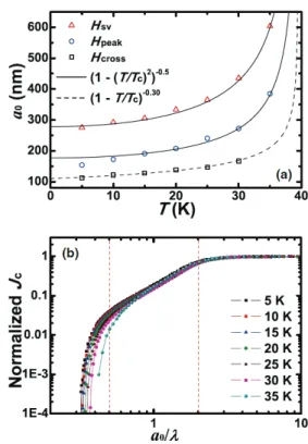
Fig. 5(a) shows the temperature dependences of the vortex lattice constant (a0) at Hsv, Hpeak, and Hcross, where Hsv is determined at the 90% of the Jc(0) at each temperature [50].
The a0 at Hsv and Hpeak shows the same temperature dependencies, denoted by the solid lines, as the penetration depth (λ) of MgB2 while the a0 at Hcross follows a different temperature dependency of (1 – T/Tc)– 0.30, denoted by the dashed line. Normalized Jc’s at 5–35 K as functions of the inter-vortex distance, where the inter-vortex distance is divided by the λ at each temperature is shown in Fig. 5(b).
The λ(0) = 100 nm and the relation λ(T) = λ(0) / [(1 – (T/Tc)2]0.5 were used to obtain λ(T) at various temperatures.
The Jc’s above α0/λ > 2 are rigid at all temperatures, but they start to decrease at α0/λ ≈ 2 because the inter-vortex interaction is strong and the weak pinning is dominant in our samples.
In addition, the curvatures of the Jc’s change again around α0/λ = 0.5 and show an exponential decay due to strong interaction between vortices. The slopes in the linear region between α0/λ ≈ 0.5- 2 re about 2–2.4 and are related to collective pinning [51]. In Fig. 5(b), the curves of the normalized Jc’s overlap up to α0 ≈λ, regardless of the number of vortices and the temperature. However, below that region, the decreasing rates become much faster with increasing temperature because of severer inter-vortex interactions and thermal fluctuation effects. These experimental results clearly show that the vortex–vortex distance, i.e., the vortex–vortex interaction, the flux pinning strength, and the temperature, are principal factors in the treatment of the Jc performance.
Fig. 6 shows normalized critical current densities at 0, 10, 29, 50, 100, and 200 mT as a function of temperature for single-crystalline MgB2 thin films. The δTc-pinning is dominant at low fields, but the pinning mechanism slowly changes to δl-pinning with increasing field at an a0 of as much as ≈2λ. The dotted lines are expected in the generalized inversion scheme (GIS) while the solid lines are expected in the modified GIS using a reasonable
Fig. 5. (a) Temperature dependences of the vortex lattice constant (a0) at Hsv, Hpeak, and Hcross. (b) Normalized Jc’s at 5–35 K as functions of the inter-vortex distance, where the inter-vortex distance is divided by the λ at each temperature.
The dashed lines are a guide for the eyes at a0 / λ = 0.5 and 2.0.
Fig. 6. Normalized critical current densities at 0, 10, 29, 50, 100, and 200mT as functions of temperature for single-crystalline MgB2 thin films. The dotted lines are expected in the generalized inversion scheme (GIS) while the solid lines are expected in the modified GIS using a reasonable penetration depth λ(t) ∝ (1 – t2) –0.5 for MgB2
instead of λ(t) ∝ (1 – t4) –0.5.
penetration depth λ(t)~(1 – t2) –0.5 for MgB2 instead of λ(t) ~ (1 – t4) –0.5. The modified GIS is quite good for describing the flux pinning mechanism of high-quality MgB2. In conclusion, the weak collective pinning was found to be dominant in single-crystalline MgB2 thin films at all temperatures, and the pinning mechanism shows a crossover from δTc-pinning to δl-pinning with increasing magnetic field.
5
A review on the understanding and fabrication advancement of MgB2 thin and thick films by HPCVD
3.2. MgB2 columnar thick films
For MgB2 polycrystalline samples, the grain boundaries are found to be the most effective pinning sources, whereas in MgB2 thin films the columnar grain boundaries are observed to be more effective pinning sites because they can interact with the flux lines over their entire length.
Kitaguchi et al. demonstrate very high critical current densities in MgB2 thin films fabricated on polished sapphire (000l) single-crystal substrates by using electron-beam evaporation technique [52]. They obtained high Jc performance due to strong flux pinning by grain boundaries between columnar grains. Using HPCVD, we fabricated MgB2 epitaxial thick films with columnar grain structures on (000l) Al2O3 substrates [33, 53].
Fig. 7(a) shows a scanning electron microscope (SEM) image of the columnar grain structure on the surface for a 1.7 µm thick film. Fig. 7(b) shows a planar-view, TEM, bright field image obtained at ~1 µm depth from the film surface. Hexagonal grain structures with an average diameter of ~300 nm can be clearly seen. The grain boundaries between these columnar grains may work as effective pinning centers, and lead to a high Jc performance for a field perpendicular to the substrate surface. Fig. 7(c) shows a cross-sectional, TEM, bright-field image. The columnar grains were in a direction perpendicular to the surface of the substrate. The in-plane selected area electron diffraction (SAED) pattern shows a zone axis of Z= [1000], as indexed in Fig. 7(d). These results indicate that the MgB2 grains have been grown along the [0001] direction.
Although most of the intercolumnar boundaries were parallel to the c-axes of the thick films, some twist-formed intercolumnar boundaries were observed on the in-plane SAED pattern, as shown Fig. 7(e).
Fig. 7. (a) SEM image of the 1.7 μm thick MgB2 film surface. (b) In-plane view of the TEM image for the 1.7 μm thick MgB2 film. (c) Cross-sectional TEM image for the 1.7 μm thick MgB2 film. (d) In-plane SAED image for the 1.7 μm thick film. (e) Out-of-plane SAED image for the1.7 μm thick film.
Fig. 8. The angular dependence of Jc for (a) M10 and (b) M14, both measured at 20 K in various magnetic fields.
JcGB is the largest at low fields, but its relative magnitude decreases with increasing field, especially above 1 T.
Fig. 9. The angular dependence of the resistivity for M14 measured at 20 K in the fields from 3.3 T to 7 T. A sharp resistive dip at θ=90° was observed up to Bc2c. The broad resistive minimum at 7 T is due to the normal state property.
Kim et al. studied the temperature and magnetic-field dependence of grain boundary pinning effect in MgB2 films with columnar grains by measuring the angular dependence of the resistivity and the critical current density (Jc) [54].
The angular dependence of Jc for two MgB2 columnar films (M10 and M14) measured at 20 K in various magnetic fields is shown in Fig. 8, where θ is defined as the angle between H and the ab plane. The systematic evolutions of the Jc(θ) in both samples with increasing magnetic field from 0.2 T to 2 T can be clearly seen, and their behaviors are basically the same to each other. There are two Jc peaks associated with H||ab and H||c, respectively. The peak at θ=0° can be understood as a result of the intrinsic pinning due to the layered structure of MgB2 [55] or/and the interface pinning. The Jc peak at θ=90° is believed to be originated in the grain boundaries of the columnar structure.
The magnetic field dependence of Jc(θ)’s at different temperatures was basically the same, only shifting the fields to lower range with increasing temperature.
6
Mahipal Ranot, P. V. Duong, A. Bhardwaj, and W. N. Kang
Interestingly, for H < 1 T at 20 K for example, JcGB s even higher than Jcab, showing that the grain-boundary flux pinning is the dominant pinning mechanism in this field range. Above 1 T, however, JcGB is smaller than Jcab, although the local peak of Jc remains even up to 3 T, indicating that the GB is still an effective pinning center at high fields. The range of the GB pinning was confirmed by the resistive dip at θ=90° even at higher fields up to Bc2.
Fig. 9 shows the angular dependence of the resistivity of M14 from 3.3 to 7 T at 20 K. A sharp resistive dip was observed at θ=90° up to 4.2 T while overall resistivity increases with fields. The existence of this resistive dip close to Bc2c indicates that the GB pinning is active as far as the superconductivity starts to nucleate. Above Bc2c, we observed a very broad minimum centered at θ=90°. This broad minimum is nothing to do with the superconductivity, but associated with the normal state property.
The field dependence of Jc for MgB2 columnar thick film is shown in Fig. 10. The self-field Jc is of the order of 107 A cm-2 at 5 K. On comparing with single-crystal like MgB2
thin film, the Jc of MgB2 film with columnar grain-boundary is much higher than that of the single-crystal like film. It indicates that grain boundaries in MgB2 do not obstruct current flow as in the high-temperature cuprate superconductors [56], but act as effective flux pinning centers like those in intermetallic superconductors, such as Nb3Sn [57].
To understand the flux pinning effect of columnar grain boundaries in columnar structured MgB2 films, the Jc was calculated at various temperatures of 5, 10, 20, 30, and 35 K. A detailed explanation on the effect of columnar grain boundaries on flux pinning in MgB2 films is given in our article [58]. Fig. 11(a) shows the magnetic field dependence of the critical current densities at temperatures of 5, 10, 20, 30, and 35 K, and the flux pinning force density (Fp) calculated from the Jc(B) data in Fig. 11(a) is shown in Fig. 11(b). The Fp’s were expressed as a function of reduced fields (b=B/B*), where B* is the critical field estimated from a Kramer plot of Jc1/2B1/4 ∝ (B*-B) (not shown here) [57]. We achieved a very high maximum flux
Fig. 10. The field dependence of Jc at 5 K for MgB2 thin film with single-crystal quality and MgB2 film with columnar grains where the magnetic field was applied parallel to the c-axis.
Fig. 11. (a) Magnetic field dependences of the critical current density (Jc) and (b) the flux pinning force density (Fp) as functions of the reduced field (b=B/B*) at temperatures of 5, 10, 20, 30 and 35 K for MB-300nm. The inset of (b) shows the temperature dependence of the maximum flux pinning force density (Fp,max), where t = T/Tc.
pinning force density (Fp,max) of 19.5 GN/m3 at 5 K, which is comparative to the theoretically estimated Fp,max (=96 GN/m3 at 4.2 K) under the assumption of full electrical connectivity of the grains. The inset of Fig. 11(b) shows the Fp,max plotted as a function of (1- t), where t (= T/Tc) is the reduced temperature. The Fp,max gradually decreases with increasing temperature, and it obeys Fp,max (1 - t)1.77, indicating the dominance of one kind of pinning source, the columnar grain boundary here, over a wide temperature region [59]. From a double logarithmic plot of Fp,max - B*, we found that the Fp,max scaled with B* according to the power law Fp,max ∝B*)1.5, and this result is similar to what was reported for polycrystals and carbon-doped MgB2
films with values of Jc(B) much higher than those of pure MgB2 samples [60, 61].
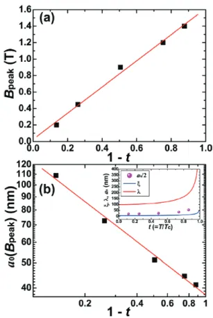
Fig. 12(a) and 12(b) present the temperature dependences of the pinning force’s peak position (Bpeak) and the vortex-vortex spacing, a0 ≈ (ϕ0/B)1/2, at given Bpeak, respectively. The Bpeak scaled as (1 - t), where t =T/Tc, and the temperature dependence of a0, as calculated from the Bpeak, was consistent with the temperature dependence of the coherence length, plotted as a0 ~ (1 – t)-0.51 ± 0.02. In this work, the a0 is defined as the average vortex-vortex spacing at Bpeak(t), where Bpeak is a specific magnetic field when the flux pinning force reaches a maximum. Using these a0
values we obtained the relationship between the a0(Bpeak) 7
A review on the understanding and fabrication advancement of MgB2 thin and thick films by HPCVD
and two superconducting characteristic lengths; coherence length (ξ) and penetration depth (λ). We plotted the temperature dependences of a0/2, the coherence length (ξ(t)
~ (1 – t)-0.5 ), and the penetration depth (λ (t) ~ (1 – t2)-0.5 ), in the inset of Fig. 12(b), where a0 is divided by the factor 2 because a0 is comparative to twice ξ and λ. Here, we used ξ(0) = 5 nm and λ(0) = 100 nm [62]. The inset of Fig. 12(b) clearly shows that the inter-vortex spacing at Bpeak(t) is related more to the coherence length than to the penetration depth, indicating that the vortices could be strongly trapped by the pinning sites, columnar grain boundaries here. If the pinning strength is weak in the samples, the Bpeak(t) would be developed at lower fields and therefore the inter-vortex spacing becomes large. These results demonstrate that flux pinning by columnar grain boundaries is not easily broken by the vortex-vortex interactions, supporting the conclusion that the columnar grain boundaries act as strong pinning sources in MgB2 films.
Kramer described the dynamic pinning force density (Fs) by flux-line lattice (FLL) shearing, which assumed synchronous shear of the FLL around pins too strong to be broken, given by the relation of Fs(b) = Ksb0.5(1 - b)2 at high fields, where the parameter Ks is related to the shear strength [63]. This formula has been widely used for scaling the flux pinning force and for estimating the
Fig. 12. (a) Temperature dependence of the Bpeak and (b) vortex-vortex spacing (a0) at each Bpeak, as calculated by using the relation of a0 ≈ (ϕo/B)1/2. The inset of (b) is a comparison of a0/2, ξ, and λ, where ξ and λ are the coherence length and the penetration depth for MgB2, respectively. Here, we used ξ(0) = 5 nm and λ(0) = 100 nm.
irreversible field or the upper critical field in superconductors having strong pinning sources [61, 64].
The values of Ks are determined from the slopes of the Fp - b0.5(1 - b)2 curves, and it scales as Ks (1 - t)1.7, which agrees with the temperature dependence of Fp,max shown in the inset of Fig. 11(b). This is a pretty clear result because the magnitude of Fp,max is largely proportional to the Ks, and this temperature dependency of Ks is related to the rigidity of the vortex lines [63, 65].
Fig. 13(a) presents the reduced field dependence of the flux pinning force densities normalized to the parameter Ks
at temperature of 5, 10, 20, 30, and 35 K. The scaling behavior is fairly fixed up to a temperature of 20 K, but the maximum size of Fp/Ks is slightly depressed at 30 and 35 K, which is due to the mean pinning strength, Kp= Ks (1 - bpeak)4 being less than the values of the Ks [63, 65].
However, the pinning force behaviors were saturated at high fields of b ≥ 0.4, indicating the dominance of a single pinning mechanism in the MB-300nm due to strong pinning sites, such as the columnar grain boundaries, despite the reduction of their effectiveness at high temperatures. Furthermore, fp as a function of B/Bpeak at temperatures of 5 – 35 K showed the different behaviors for
Fig. 13. (a) Reduced field dependences of the flux pinning force density normalized to the parameter Ks, and (b) normalized flux pinning force density fp(= Fp/Fp,max) as a function of the magnetic field normalized to Bpeak at temperatures of 5, 10, 20, 30, and 35 K for MgB2 columnar thick film. The curves show a change in the pinning force behavior at temperatures above 20 K, indicating a slight depression of the pinning effect in columnar grain boundaries due to thermal fluctuation effects.
8
Mahipal Ranot, P. V. Duong, A. Bhardwaj, and W. N. Kang
B/Bpeak > 1, as shown in Fig. 13(b). The rates of decrease of fp(B/Bpeak) are approximately the same at 5 and 10 K, but slowly become faster with increasing temperature for temperatures above 20 K. On the basis of these results, we suggest that the columnar grain boundaries in MgB2 films act as strong pinning centers and contribute as the main pinning source over a wide range of temperatures, even though their effectiveness is depressed at temperatures above 20 K.
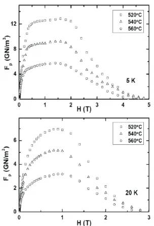
An unusual double-peak behavior was also observed for the pinning-force density in MgB2 thick films with columnar structures [53]. Magnetic-field dependences of the flux pinning force density (Fp) for MgB2 thick films at 5 and 20 K is shown in Fig. 14. This double-peak behavior of the pinning forces does not obey any flux pinning scaling laws, but could be well scaled by using separate pinning forces with the reduced irreversible fields bH = H/Hirr and bL = H/H*. A complete analysis and explanation on the possible origin of double-peak behavior of the pinning-force density in thick MgB2 films with columnar structures is provided in the Ref. [53]. We divided the double peaks with another irreversible field (H*), to interpret the two types of pinning sources. The pinning forces separated by each irreversible field, bH = H/Hirr and bL = H/H* are well scaled with a functional form fp∝bp(1 - b)q, implying that these double-peak features are related to, at least, two different pinning mechanisms, such as point defects and grain boundaries with columnar grains.
Fig. 14. Magnetic-field dependences of the flux pinning force density (Fp) for MgB2 columnar thick films at 5 and 20 K. The enhancement of Fp with decreasing grain size is obvious.
Furthermore, the double-peak features decreased with increasing temperature whereas the shape of the graph in the high reduced field region (bH ≥ 0.29) remained unchanged. These results directly suggest that the flux pinning mechanism due to columnar grain boundaries should be dominant in MgB2 thick films and should play a crucial role in enhancing the Jc over a wide range of magnetic fields and temperatures.
3.3. a-axis-oriented MgB2 films
There are two types of flux pinning: intrinsic pinning and extrinsic pinning. To improve the field performance of Jc, in general, many researchers have used extrinsic pinning methods, such as chemical doping [66], nanoparticle addition [67], heavy-ion [68] or neutron irradiation [69], reducing grain size to enhance grain boundary pinning sites [70] and so on. Among these various efforts, reducing the grain size [70] and carbon doping [66] are known to be the most effective ways to improve pinning properties in MgB2. Nevertheless, further progress in the critical current density is needed for real applications. We have developed another effective method for the improvement of Jc in MgB2. The focus has moved to intrinsic pinning instead of the already much studied extrinsic pinning. The intrinsic pinning generally shows angular dependence due to the anisotropy of the material, which is prominently observed in
Fig. 15. (a) Comparison of XRD patterns of highly c-axis-oriented single-crystalline MgB2 film, MgB2-(A), and a-axis-oriented MgB2 film, MgB2-(D). (b) XRD patterns for MgB2 films of thicknesses 0.6 and 2.0 μm. The orientation of grains changed from c-axis to a-axis on increasing the thickness of the MgB2 film.
9
A review on the understanding and fabrication advancement of MgB2 thin and thick films by HPCVD
Fig. 15. (a) Comparison of XRD patterns of highly c-axis-oriented single-crystalline MgB2 film, MgB2-(A), and a-axis-oriented MgB2 film, MgB2-(D). (b) XRD patterns for MgB2 films of thicknesses 0.6 and 2.0 μm. The orientation of grains changed from c-axis to a-axis on increasing the thickness of the MgB2 film.
high-temperature superconductors (HTS) with a layered structure [71]. HTS has a weak superconducting region between the CuO2 planes and the vortices can be pinned to them intrinsically. Similarly, MgB2 also has a layered structure, and it is described as a two-band superconductor with two gaps of Δσ and Δπ coming from boron px,y orbitals and boron pz orbitals, respectively. Moreover, Takahashi et al. [55] reported the exhibition of intrinsic pinning in single-crystalline MgB2 by measuring the magnetic torque, and it originates from boron planes which act as the main superconducting layers in MgB2. The c-axis coherence length in MgB2 is about 5 nm and even larger in the a-b plane. This suggesting that the longer coherence length a-b films are more advantageous for superconducting electronics applications.
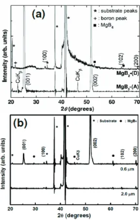
The fabrication of c-axis and a-axis oriented HPCVD MgB2 films on c-cut Al2O3 substrates was controlled by changing the concentration of diborane (B2H6) gas and substrate temperature [72]. Fig. 15(a) shows X-ray diffraction (XRD) patterns of θ–2θ scans of single-crystalline MgB2 film, MgB2-(A), and a-axis-oriented MgB2 film, MgB2-(D). XRD data of MgB2-(A) indicates that this film is highly c-axis oriented without any impurity peak. On the other hand, the preferred orientation of MgB2-(D) is not c axis and the component of
Fig. 16. Plane-view SEM images for MgB2 films of (a) single-crystalline MgB2 film, (b) MgB2 columnar film, (c) a-axis-oriented MgB2 film, and (d) a-axis-oriented MgB2
film.
c-axis orientation is only seen in the (102) peak. In addition, the XRD peaks of (100) and (200) in MgB2-(D) represent that the c-axis grains of this film are oriented parallel to the substrate surface. We also have controlled the grain growth orientation of MgB2 by varying the thickness of the MgB2
film at fixed B2H6 gas concentration and substrate temperature [73]. The grain growth orientation was found to change from c-axis to a-axis on increasing the thickness of the MgB2 film as shown in Fig. 15b.
Fig. 16 shows the surface morphologies of (a) single-crystalline MgB2 film, MgB2-(A), (b) MgB2
columnar film, MgB2-(B), (c) a-axis-oriented MgB2 film, MgB2-(C), and (d) a-axis-oriented MgB2 film, MgB2-(D).
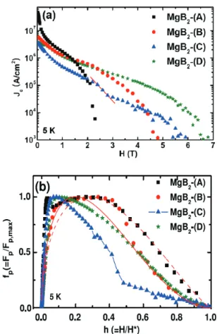
The field dependence of Jc at 5 K for different kinds of films, single-crystalline film, MgB2 columnar film, and two a-axis-oriented MgB2 films are shown in Fig. 17(a). The superior critical current properties were observed for a-axis oriented MgB2 films at high fields compared with c-axis-oriented films, even though the flux pinning by columnar grain boundaries in MgB2-(B) is stronger than grain boundary pinning in MgB2-(C) and MgB2-(D). This result comes from the anisotropy of intrinsic pinning, which provides new information for the superior field performance of Jc. These results suggest that by fabricating highly a-b-axis oriented MgB2 films high Jc performance over a wide magnetic field region could be obtain.
Furthermore, if this method is applied to fabricate MgB2
coated conductors, superior results can be expected in large-scale applications.
We tried to scale the flux pinning force density (Fp) in order to further investigate the pinning mechanism for the four kinds of MgB2 films. The normalized flux pinning force density, fp(=Fp/Fp,max), versus reduced magnetic field, h(= H/H*), for all films is shown in Fig. 17(b). In the case of the single-crystalline sample of MgB2-(A), the normalized flux pinning force fp(h) is scaled well by the relation of fp(h)
∝ h0.5(1 − h)1.3, plotted by the dashed line as shown in Fig.
17(a) and (b). This relation is close to the scaling formula 10
Mahipal Ranot, P. V. Duong, A. Bhardwaj, and W. N. Kang
Fig. 17. (a) Magnetic field dependences of the critical current density for MgB2 films of MgB2-(A), MgB2-(B), MgB2-(C) and MgB2-(D) at 5 K. (b) Scaling behavior of the normalized flux pinning force density, fp(= Fp/Fp,max), versus reduced magnetic field, h(= H/H*), for four kinds of MgB2 films.
for flux pinning, fp(h) ∝ h0.5(1 − h), originating from weak dislocations. Weak dislocations were observed to be the main defects in MgB2-(A) by using a transmission electron microscope (TEM) and two-beam conditions [74]. On the other hand, the fp(h) data for MgB2-(B) and (D) at 5 K were scaled by the relation of fp(h) ∝ h0.5(1 − h)2 in the high field regions in which only a strong pinning mechanism could be considered, such as planar defects. The data is difficult to describe perfectly within the context of the proposed scaling models for flux pinning, but the data for MgB2-(D) without c-axis orientation are fairly well consistent with the scaling model considered for strong pinning sources, suggesting that the boron layers in MgB2 play a crucial role in strong intrinsic pinning.
4. DOPING / IMPURITY EFFECT ON Jc
The practical applications of any superconductor strongly depend on its capacity for carrying loss-free currents in high magnetic fields [23, 75]. The Jc of MgB2
drops rapidly with increasing magnetic field due to its poor flux pinning. The large scale electric power applications have been hampered so far by the poor flux pinning
behavior of MgB2 which induces the degradation of Jc in high magnetic fields. Pinning of vortices can be achieved by creating pinning sites such as point defects, planar defects and impurities. An intensive research has been done on the enhancement of Jc in MgB2 bulk, wires and tapes, however, only little work has been reported on improving the Jc in MgB2 films. Researchers have attempted to improve the flux pinning of MgB2 thin films through proton [68] and neutron irradiation [69]. However, for practical applications, the pinning centers should be introduced by a simple process, such as chemical doping. Chromic et al.
[76] fabricated MgB2 thin films on SiC buffered Si substrates by sequential electron beam evaporation. Yao et al. [77] reported very thick MgB2 films (60–140 μm) doped with SiC nanoparticles on Ni substrates processed using a very short-time in situ reaction. Other kinds of layered structures, such as MgB2/Mg2Si multilayers [78] and MgB2/Ni multilayers [79], were also examined for Jc
enhancement. HPCVD system was also employed to explore the flux pinning properties and to improve the Jc
performance of MgB2 films through doping and impurity additions. The various attempts performed by using HPCVD are discussed below.
4.1. Effect of Ag-impurity layers
We demonstrated a simple method for the enhancement of Jc in MgB2 thick films with amorphous Ag-impurity layers. Firstly, Ag-impurity layers were deposited on c-cut Al2O3 substrates at room temperature using pulsed laser deposition (PLD) technique. Subsequently, MgB2 films were grown on top of Ag/Al2O3 at 560 and 600 °C by using HPCVD. A detailed description on fabrication and the effect of Ag doping in MgB2 films can be found elsewhere [80]. Since the binding energy of the amorphous phase is lower than that of the crystal phase, the melting temperature (TM) of an amorphous state material is much lower than that of a crystallized material. For instance, glass has a TM ≥ 300 °C, while for quartz, TM ~ 1650 °C. In the light of this, we fabricated Ag doped MgB2 films using an amorphous Ag layer at low growth temperatures.
Fig. 18(a) shows the magnetic field dependence of Jc at 5 and 20 K for pure and MgB2 films fabricated on various Ag-impurity layers. All Jc (H) curves of Ag-doped MgB2
films have much higher Jc than that of pure MgB2 film over the whole field region. The enhancement in Jc is likely the effect of improved flux pinning by grain boundaries and additional pinning sites created by Ag-impurity layers. The optimal thickness of Ag-impurity layer for the enhancement of Jc in MgB2 film is observed to be 16 nm. At 5 K and 1 T, this film has a Jc value three times higher than the pure MgB2 film. However, an even more interesting and significant result obtained at high fields is that, for the relatively small amount of defects introduced by 4-nm-thick Ag layer, shows higher Jc than the other Ag-doped films. The high Jc at higher fields is mainly due to strong flux pinning by high density of grain boundaries in Ag-doped MgB2 film with 4 nm in thickness.
11
A review on the understanding and fabrication advancement of MgB2 thin and thick films by HPCVD
Fig. 18. Effect of Ag-impurity layers on the magnetic field dependence of Jc and flux pinning properties. (a) Jc(H) curves of pure and MgB2 films grown on various Ag-impurity layers at 5 K (solid symbols) and 20 K (open symbols). (b) The normalized flux pinning force density against the reduced magnetic field at 5 and 20 K for Ag-doped MgB2 films. The solid line is fitting to the theoretical function fp∝ bp(1-b)q , where p=0.48 and q=1.62.
The normalized flux pinning force density, fp=Fp/Fp,max, as a function of reduced magnetic field, b=H/Hirr, for Ag-doped MgB2 films at 5 and 20 K are plotted in Fig.
18(b). As we can see, the peak of fp(b) curves shifts towards the lower reduced field with decreasing temperature. This behavior strongly suggests that different kinds of pinning centers, such as grain boundaries and other defects (i.e., MgAg, intragrain defects or non-superconducting particles like MgB4 and Mg) are present in the samples. This result is in contrast with previously reported data in reference [81], where they obtained the shift in peak position of fp(b) with doping level, whereas independent of temperature. A shift in the peak of fp(b) curves could be attributed to the increase in the density of defects at a low temperature of 5 K, as their pinning strength becomes weak or less effective at higher temperature due to thermal effect. Moreover, fp(b) data curves at 5 K, do not even show a bell like shape and are not able to be fit with any proposed theoretical function.
The lack of fitting of scaled fp(b) data at 5 K, also indicates the existence of additional pinning sites. The scaled data at 20 K is reasonably fitted to the theoretical functional form fp∝ bp(1-b)q with p=0.48 and q=1.62, and the peak in fp
occurs at a reduced field of b≈0.23. These observations
Fig. 19.The Jc (H) curves at 5 K for Ag and Cu-doped MgB2 thick films grown at 560 ºC on 8 and 16-nm-thick impurity layers of Ag (solid symbols) and Cu (open symbols), respectively
indicate that the flux pinning force density (Fp) comes from flux pinning by grain boundaries and by the presence of other type of defects as a consequence of Ag doping.
4.2. Effect of Cu-impurity layers
The influence of the thickness of Cu-impurity layers on microstructure and Jc of MgB2 thick films was also investigated [82]. A significant enhancement in the critical current density at low field region was obtained for Cu-doped films as compared to pure MgB2 film (not shown here). Fig. 19 shows the comparison of magnetic field dependence of Jc at 5 K between the Ag and Cu-doped MgB2 films fabricated at a temperature of 560 °C. The Ag doping was found to be more effective than the Cu doping for Jc enhancement in MgB2 films, indicate that Ag is likely to be a promising flux pinner in MgB2 superconductor.
4.3. Effect of amorphous SiC-impurity layers
The SiC is known to be the best dopant for enhancing Jc and Hc2 in superconducting MgB2 [83]. Dou et al. [66] explained how the doped SiC nanoparticles influence MgB2 on the basis of the dual-reaction mechanism. According to the dual-reaction model, SiC nanoparticles which react with Mg at temperatures above 600 °C form Mg2Si compounds. The remaining free carbon (C) atoms are substituted into the boron (B) sites. In this process, SiC nanoparticles create strong pinning centers in MgB2 leading to good Jc performance under high magnetic fields. We have fabricated the superconducting MgB2 films grown on amorphous SiC-impurity layers of different thickness by means of the HPCVD and PLD method, details can be found in [84].
Fig. 20 shows the critical current density (Jc) versus applied magnetic field at 5 and 20 K for pure and SiC doped MgB2 thick films fabricated on c-cut Al2O3
substrates. The SiC 35 nm MgB2 thick film had the highest Jc among all the samples and the SiC doped samples using impurity layers showed a higher Jc than the pure MgB2
thick film over the whole magnetic field region. These results indicate that the 35 nm thick SiC impurity layer has
0 1 2 3 4 5
104 105 106 107
MgB2 560oC/Ag or Cu/Al2O3
T = 5 K Ag 8nm Ag 16nm Cu 8nm Cu 16nm
H (T) Jc(A/cm2 )
12
Mahipal Ranot, P. V. Duong, A. Bhardwaj, and W. N. Kang
Fig. 20. The critical current density (Jc) versus applied magnetic field at 5 and 20 K for pure and SiC doped MgB2
thick films. The SiC 35 nm sample has the highest Jc and all SiC doped samples show a higher Jc than the pure MgB2
thick film over the whole applied magnetic field region.
the optimal thickness for the enhancement of Jc at a low growth temperature of 480 °C. The low-temperature growth deposition is very important for fabrication of MgB2 coated-conductor, tape, wire, and film to protect the reactions between MgB2 and other materials, such as flexible metallic substrates. At zero fields, all SiC doped samples show higher Jc than the pure MgB2 film, indicating that the inter-grain connectivity of SiC doped films is denser than that of the pure ones. These results suggest that the SiC particles of the impurity layer diffused into the MgB2 films during film growth, and the SiC particles, along with the columnar grain boundaries in the MgB2 thick films, act as strong pinning centers.
4.4. Effect of crystalline SiC-buffer layers
The recent study on SiC-doping in MgB2 by Zeng et al.
reported that the SiC in its crystalline form behaves very differently than the amorphous form [85]. They prepared SiC-MgB2 composite by the diffusion process. In contrast to chemical doping effects, they observed the thermal stress/strain as a source of strong flux pinning center when there is no reaction between SiC and MgB2. Both the Jc and Tc are improved by the thermal strain on the interface between SiC and MgB2 during the diffusion process. The enhancement is attributed to the difference in the thermal expansion coefficient between SiC and MgB2, which can create thermal strain in the MgB2 matrix during cooling.
Large strains could be expected in the films form when one layer is deposited on the other.
Byeongwon et al. studied the effect of crystalline SiC-buffer layers on the flux pinning behavior of MgB2
films fabricated on c-cut Al2O3 substrates [86, 87]. The result of Jc for pure and SiC-buffered-MgB2 films when subjected to an applied magnetic field is showed in Fig. 21.
It is evident that for all of the SiC-buffered-MgB2 samples, the Jc-H behavior at both temperatures of 5 and 20 K has been significantly improved with the addition of SiC-buffer layers. At the same time, the degradation of Jc with increasing magnetic field becomes slow. Among all
Fig. 21. Effect of SiC-buffer layers on the field dependence of critical current density (Jc) curves measured at (a) 5 and (b) 20 K for pure and SiC-buffered-MgB2 films. The SiC-buffered-MgB2 samples show larger Jc values than those of pure MgB2 at whole field region with SiC 120 nm showing the highest Jc enhancement for both 5 and 20 K temperatures.
samples, MgB2 film with 120 nm thick-SiC-buffer layer showed the highest Jc values. The enhancement of Jc values in crystalline SiC-buffered layers MgB2 is well above the Jc
enhancement obtained with amorphous SiC-impurity layers [84]. They have studied the local structure of MgB2 films grown on SiC buffer layers by extended X-ray absorption fine structure (EXAFS) spectroscopy [88]. It was found that as SiC-buffer layers thicken the ordering of Mg–B and Mg–Mg bonds of MgB2 films began to change, indicating SiC buffer layers significantly altered the local structure of MgB2 films.
4.5. Effect of carbon-doping
The substitution of carbon atoms into the boron sites of MgB2 are known to be the most effective way to improve flux pinning properties in MgB2 and hence Jc performance under high magnetic fields. The current-carrying performance has been improved by carbon in all the form of MgB2 superconductors, such as polycrystalline bulk, single crystals, wires, tapes, filaments, fibers and thin films.
In contrast to MgB2 bulks and single crystals, where the substitution of carbon for boron site seems easy, but is rather challenging to dope carbon in MgB2 films, though only a little work has been reported [25, 61]. In carbon-alloyed MgB2 films made by HPCVD using a metal–organic (MeCp)2Mg (MO)as the carbon source, Hc2
has been raised to above 60 T [25, 89]. A TEM study proposed that the c-axis tilt in these carbon-alloyed MgB2
13