Progress in Superconductivity and Cryogenics
Vol.15, No.2, (2013), pp.9~11 http://dx.doi.org/10.9714/psac.2013.15.2.009
```
1. INTRODUCTION
MgB
2superconductor is a very promising material for practical applications because of its unique properties, such as simple crystal structure, high transition temperature (40 K), high self-field critical current density (J
c), existence of two gaps, the strongly linked nature of the intergrains, and low cost [1, 2]. Inspite of its high self-field J
c, J
cdrops rapidly in high magnetic fields due to poor flux pinning. To increase the potential use of MgB
2superconductor in practical applications, enhancements in the critical current density under high magnetic fields is essential. Some of these applications include superconducting magnets and solenoids, microelectronic devices and coated conductor wires for power applications. In these applications, strong pinning of vortices is an important requirement for operation with low noise and lower power loss. Pinning of vortices can be achieved intrinsically and extrinsically.
Extensive research has already been carried out to improve the flux pinning in MgB
2by extrinsic methods, such as chemical doping, nanoparticles addition, and proton or neutron irradiation etc [3, 4]. Takahashi et al. reported the evidence of intrinsic pinning in MgB
2by measuring the magnetic torque of a single-crystalline MgB
2when the field is applied parallel to the boron layers [5]. Recently, we have reported on the intrinsic pinning effect in three kinds of MgB
2superconductors, such as c-axis-oriented single crystal film, c-axis-oriented columnar structure film and
films without c-axis orientation perpendicular to the substrate surface [6]. Those films were deposited under different experimental conditions by using hybrid physical chemical vapor deposition (HPCVD) technique. It is observed that the flux pinning behavior and overall J
cof the films critically depend on the experimental conditions.
Therefore, in this study, MgB
2films are fabricated on c-cut Al
2O
3substrates under the same experimental conditions except the thickness of MgB
2films. The influence of thickness on the grain growth direction and on the super- conducting properties of MgB
2films was investigated.
2. EXPERIMENTAL
MgB
2films of various thicknesses 0.6, 0.9, 1.4 and 2.0 µm with different orientation of grains were deposited on
c-cut Al2O
3substrates (10 mm × 10 mm in size) by using HPCVD. In contrast to our previous work, where MgB
2grain growth orientation was controlled by changing the concentration of diborane (B
2H
6) gas and substrate temperature (T
s) [6], in the present work, it is controlled by varying the thickness of the MgB
2film at a fixed B
2H
6gas concentration and substrate temperature. The concen- tration of B
2H
6gas, having originally been 5%, is tuned by mixing with high purity (6N) hydrogen (H
2) gas. All the films of thicknesses 0.6, 0.9, 1.4 and 2.0 µm were deposited at a temperature of 540
oC. The thicknesses of MgB
2/Al
2O
3films were examined by scanning electron microscopy (SEM). A detailed description of the growth process for
Thickness dependence of grain growth orientation in MgB 2 films fabricated by hybrid physical-chemical vapor deposition
Mahipal Ranot and W. N. Kang*
BK21 Physics Division and Department of Physics, Sungkyunkwan University, Suwon, Korea (Received 23 May 2013; revised or reviewed 26 June 2013; accepted 27 June 2013)
Abstract
We have investigated the effect of thickness of the MgB2 film on the grain growth direction as well as on their superconducting properties. MgB2 films of various thicknesses were fabricated on c-cut Al2O3 substrates at a temperature of 540 °C by using hybrid physical-chemical vapor deposition (HPCVD) technique. The superconducting transition temperature (Tc) was found to increase with increase in the thickness of the MgB2 film. X-ray diffraction analysis revealed that the orientation of grains changed from c-axis to a-axis upon increasing the thickness of the MgB2 film from 0.6 to 2.0 µm. MgB2 grains of various orientations were observed in the microstructures of the films examined by scanning electron microscopy. It is observed that at high magnetic fields the 2.0-µm-thick film exhibit considerably larger critical current density (Jc) as compared to 0.6-µm-thick film. The results are discussed in terms of an intrinsic-pinning in MgB2 similarly as intrinsic-pinning occurring in high-Tc cuprate superconductors with layered structure.
Keywords : MgB2 film, grain orientation, HPCVD
* Corresponding author: [email protected]
Thickness dependence of grain growth orientation in MgB2 films fabricated by hybrid physical-chemical vapor deposition
MgB
2films by using HPCVD can be found in our previous report [7].
The resistivity measurements were carried out on all the MgB
2films by the standard four-probe method. The crystal structure of the films were investigated by X-ray diffraction (D8 discover, Bruker AXS) using Cu Kα as an X-ray source. The surface morphology and thickness were measured by scanning electron microscopy (SEM). The magnetization hysteresis (M −
H) measurements werecarried out on all the films using a magnetic property measurement system (Quantum Design MPMS).
3. RESULTS AND DISCUSSION
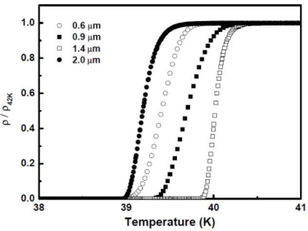
The temperature dependences of the normalized resistivity for the MgB
2/Al
2O
3films of various thicknesses 0.6, 0.9, 1.4 and 2.0 µm are plotted in Fig. 1. The MgB
2films have superconducting transition temperature (T
c) ranging between 39.4 and 40.1 K with superconducting transition width (∆T
c) of 0.2 – 0.4 K. The T
cwas found to increase with the increase in the film thickness, and reached its maximum value of 40.1 K for 1.4-µm-thick film, above which it starts to decrease. The increase in T
cis most probably due to the tensile strain in the films which reported to be the possible cause of higher T
cin MgB
2films, and the thicker the film the larger the tensile strain [8]. The 2.0-µm-thick film has a T
cof 39.4 K which is comparable with the previously reported a-axis-oriented MgB
2films [6].
Fig. 2 shows the X-ray diffraction patterns (XRD) for MgB
2films of thicknesses 0.6 and 2.0 µm. It is observed that the 0.6-µm-thick MgB
2film has a preferred orientation along the (00l) plane in addition to small diffraction peaks of (100), (102) and (200) of different MgB
2planes. The 0.9-µm-thick MgB
2film also has a similar XRD data as 0.6-µm-thick film with preferred orientation along the (00l)
Fig. 1. Temperature dependences of the normalized resistivity of MgB
2/Al
2O
3films of various thicknesses 0.6, 0.9, 1.4 and 2.0 µm fabricated at 540
oC.
Fig. 2. X-ray diffraction patterns for MgB
2films of thicknesses 0.6 and 2.0 µm. The orientation of grains changed from c-axis to a-axis on increasing the thickness of the MgB
2film.
plane. We found that with increasing the thickness of the MgB
2film the peak intensities of c-axis oriented diffraction peaks become weak, and almost disappear for thickness of 2.0 µm. In other words, the orientation of grains changed from c-axis to a-axis upon increasing the thickness of film.
The impurity peaks of MgB
4were observed in all the films as were noticed in our previous report on differently oriented MgB
2films [6].
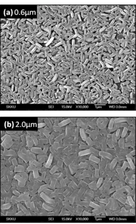
The surface morphologies of MgB
2/Al
2O
3films were examined by scanning electron microscopy (SEM). The SEM images of MgB
2films of thicknesses 0.6 and 2.0 µm are shown in Figs. 3a and 3b. Grains of various orientations could be seen in both the SEM images, which is consistent with XRD results. In addition, the MgB
2grains of 2.0-µm-thick film, Fig. 3b, are well connected and have a dense microstructure as compared to the grains of thinner film, Fig. 3a. It indicates that thick MgB
2layer results in compact and dense microstructure.
The critical current density (J
c) of all the films was estimated from magnetization hysteresis loops using the Bean’s critical state model [9]. The magnetic field dependence of J
cat 5 K for MgB
2films of thicknesses 0.6 and 2.0 µm with different orientation of grains are shown in Fig. 4. The 0.6-µm-thick MgB
2film shows higher J
cat self- field and in the low field region which is similar to the highly c-axis-oriented film as reported before [10].
Whereas, a crossover of the J
c(H) at 2.3 T was observed for the a-axis-oriented MgB
2film of thickness 2.0 µm when compared to the 0.6-µm-thick film. At high magnetic fields the 2.0-µm-thick film (without c-axis orientation) exhibit considerably larger critical current density. This result is attributed to an intrinsic-pinning anisotropy in MgB
2as we observed before for MgB
2films with different c-axis orientations [6]. The present results also show that MgB
2exhibits strong intrinsic pinning in the in-plane direction
10
Mahipal Ranot and W. N. Kang
Fig. 3. The surface morphologies of MgB
2/Al
2O
3films of thicknesses (a) 0.6 µm and (b) 2.0 µm deposited at 540
oC.
The thicker film has a denser microstructure as compared to the thinner one.
Fig. 4. The critical current density as a function of magnetic field measured at 5 K for MgB
2films of thicknesses 0.6 and 2.0 µm.
caused by the large superconducting energy gap in the ab plane like high-T
ccuprate superconductors with a layered structure [11].
4. CONCLUSION
In summary, MgB
2films of various thicknesses were deposited on c-cut Al
2O
3substrates by using hybrid
physical–chemical vapor deposition (HPCVD) technique.
The effect of thickness of the MgB
2film on the grain growth direction as well as on the superconducting properties of MgB
2films was studied. It was found that the orientation of grains changed from c-axis to a-axis on increasing the thickness of the MgB
2film. MgB
2grains of various orientations were observed in all the films by SEM analysis. At high fields the 2.0-µm-thick film showed considerably larger critical current density as compared to 0.6-µm-thick film. These findings suggest that the HPCVD is capable of producing highly c-axis and a-axis-oriented films which would be very promising for the fabrication of high J
cMgB
2wires and tapes for practical applications.
ACKNOWLEDGMENT
This work was supported by Mid-career Researcher Program through National Research Foundation of Korea (NRF) grant funded by the Ministry of Education, Science
& Technology (MEST) (No. 2010-0029136).
REFERENCES
[1] W. N. Kang, H. J. Kim, E. M. Choi, C. U. Jung and S. I. Lee, "MgB2
superconducting thin films with a transition temperature of 39 Kelvin," Science, vol. 292, pp. 1521, 2001.
[2] K. Vinod, R. G. A. Kumar and U. Syamaprasad, "Prospects for MgB2 superconductors for magnet application," Supercond. Sci.
Technol., vol. 20, pp. R1, 2007.
[3] W. K. Yeoh and S. X. Dou, "Enhancement of Hc2 and Jc by carbon-based chemical doping," Physica C, vol. 456, pp. 170, 2007.
[4] R. H. T. Wilke et al., "Superconducting and normal state properties of carbon doped and neutron irradiated MgB2," Physica C, vol. 456, pp. 108, 2007.
[5] K. Takahashi, T. Atsumi, N. Yamamoto, M. Xu, H. Kitazawa and T.
Ishida, "Superconducting anisotropy and evidence for intrinsic pinning in single crystalline MgB2," Phys. Rev. B, vol. 66, pp.
012501, 2002.
[6] Soon-Gil Jung, N. H. Lee, W. K. Seong, K. H. Cho, W. N. Kang and S. Oh, "Observation of strong intrinsic pinning in MgB2 films,"
Supercond. Sci. Technol., vol. 24, pp. 075003, 2011.
[7] Mahipal Ranot and W. N. Kang, "MgB2 coated superconducting tapes with high critical current densities fabricated by hybrid physical-chemical vapor deposition," Curr. Appl. Phys., vol. 12, pp.
353, 2012.
[8] A. V. Pogrebnyakov et al., "Enhancement of the superconducting transition temperature of MgB2 by a strain-induced bond-stretching mode softening," Phys. Rev. Lett., vol. 93, pp. 147006, 2004.
[9] D. X. Chen and R. B. Goldfarb, "Kim model for magnetization of type-II superconductors," J. Appl. Phys., vol. 66, pp. 2489, 1989.
[10] W. K. Seong, S. Oh and W. N. Kang, "Perfect domain-lattice matching between MgB2 and Al2O3: single-crystal MgB2 thin films grown on sapphire," Jpn. J. Appl. Phys., vol. 51, pp. 083101, 2012.
[11] B. Roas, L. Schultz and G. Saemann-Ischenko, " Anisotropy of the critical current density in epitaxial YBa2Cu2Ox films," Phys. Rev.
Lett., vol. 64, pp. 479, 1990