글로벌 배선 적용을 위한 UV 패턴성과 UV 경화성을 가진 폴리실록산
송창민1·박해성2·서한결3·김사라은경1,†
1서울과학기술대학교 나노IT디자인융합대학원, 2서울과학기술대학교 일반대학원 기계공학과,
3서울과학기술대학교 정보통신대학 전자IT미디어공학과
Organic-inorganic Hybrid Dielectric with UV Patterning and UV Curing for Global Interconnect Applications
Changmin Song1, Haesung Park2, Hankyeol Seo3, and Sarah Eunkyung Kim1,†
1Graduate School of Nano-IT Design Convergence, Seoul National University of Science and Technology, 232, Gongneung-ro, Nowon-gu, Seoul 01811, Korea
2Department of Mechanical Engineering, Seoul National University of Science and Technology, 232, Gongneung-ro, Nowon-gu, Seoul 01811, Korea
3Media IT Engineering Program, Seoul National University of Science and Technology, 232, Gongneung-ro, Nowon-gu, Seoul 01811, Korea
(Received October 30, 2018: Corrected December 20, 2018: Accepted December 24, 2018)
Abstract: As the performance and density of IC (integrated circuit) devices increase, power and signal integrities in the global interconnects of advanced packaging technologies are becoming more difficult. Thus, the global interconnect technologies should be designed to accommodate increased input/output (I/O) counts, improved power grid network integrity, reduced RC delay, and improved electrical crosstalk stability. This requirement resulted in the fine-pitch interconnects with a low-k dielectric in 3D packaging or wafer level packaging structure. This paper reviews an organic- inorganic hybrid material as a potential dielectric candidate for the global interconnects. An organic-inorganic hybrid material called polysiloxane can provide spin process without high temperature curing, an excellent dielectric constant, and good mechanical properties.
Keywords: Dielectric, PSSQ, Global Interconnect, UV Curing, Metallization
1. 서 론
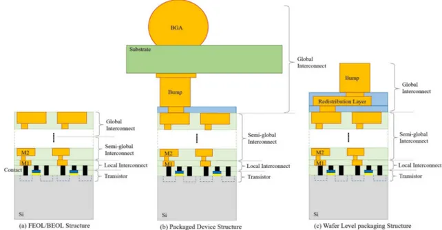
반도체 소자의 트랜지스터 기술은 non-planar CMOS 구 조와 기생 저항(parasitic resistance)과 기생 커패시턴스 (parasitic capacitance) 감소를 위한 지속적인 연구에도 불 구하고 점차 물리적 한계에 도달하고 있다.1) 그리고, 소 자의 급격한 성능 향상과 밀도 증가는 배선 기술의 향상 을 지속적으로 요구하고 있고, 로컬 배선보다는 글로벌 배선 기술 향상이 더욱 중요해지고 있다. 반도체 소자의 배선 구조는 일반적으로 전공정 배선과 패키징 배선으로 나뉜다. Fig. 1(a)와 같이 전공정 내 배선은 일반적으로 3 부분으로 나누고, W plug(contact)와 M1(첫번째 금속 배 선)을 로컬 배선(local interconnect), M2에서 M4를 세미글 로벌 배선(semi-global interconnect), 그리고 M5 이후를 글
로벌 배선(global interconnect)이라 부른다. 하지만, 패키 지된 소자 전체 구조를 볼 때 배선은 Fig. 1(b)와 같이 전 공정 내 배선을 로컬 배선과 세미글로벌 배선으로 나누 고, 범프(bump)부터 이후 패키징 배선을 글로벌 배선으 로 보기도 한다. 최근 각광을 받고 있는 웨이퍼 레벨 패 키징(wafer level packaging) 구조(Fig. 1(c))의 재배선 층 (redistribution layer) 또한 글로벌 배선이라고 칭할 수 있 다. 본 연구에서는 Fig. 1(b)와 (c)에서와 같이 패키지 영 역에서의 배선을 글로벌 배선이라 정의하도록 하겠다.
배선의 성능을 결정하는 주요 성능지표(performance metric)는 RC Delay이고, Fig. 2에서 보듯이 소자가 scaled- down 될수록 배선의 길이는 길어지고 선폭은 좁아져서 RC Delay 시간이 증가하고 있다.2-5) 특히 현재 소자의 시 스템 성능은 글로벌 배선의 영향이 가장 큰 것으로 나타
†Corresponding author
E-mail: [email protected]
© 2018, The Korean Microelectronics and Packaging Society
This is an Open-Access article distributed under the terms of the Creative Commons Attribution Non-Commercial License(http://creativecommons.org/
licenses/by-nc/3.0) which permits unrestricted non-commercial use, distribution, and reproduction in any medium, provided the original work is properly cited.
특집 : Hybrid Spin Dielectric for Global Interconnects
나고 있다. 배선 길이가 증가하고 선폭이 좁아지면 RC Delay의 증가뿐 아니라 전력(power)도 증가하고 누화 (crosstalk) 현상도 발생하게 되어 전기적 신뢰성에 문제 를 야기한다.6)이에 배선에서 저항(R, resistance)과 커패 시턴스(C, capacitance, eq)의 조절은 매우 중요한 요소가 된다. 금속 라인의 경우 낮은 전기 저항과 좋은 오믹 (ohmic) 접촉, 그리고 EM(electromigration)과 같은 전기적 신뢰성 문제에 강해야 하며, Al 라인에서 Cu 라인으로 발 전해 왔고 최근에는 Ru이나 Co가 각광을 받고 있다. 유 전체(dielectric)의 경우 낮은 유전상수와 열적, 기계적 안 정성이 있어야 하며 경우에 따라서는 우수한 금속 스텝 커버리지(step coverage)가 요구되기도 한다. 유전체의 유 전상수를 낮추려면 유전체 소재의 극성(polarization)을 낮 추거나 밀도를 낮추어야 한다.7,8) Table 1에서 보듯이 전공 정 배선 공정에서는 고분자 유전체도 연구가 되었으나, 주 로 SiO2 박막이 유전체로 사용되어 왔으며, SiO2 박막 내 Si-O의 밀도를 낮추거나 F 또는 C를 도핑(doping)하는 방
법이 주로 적용되었다.9-10)패키징 분야인 글로벌 배선 공 정의 경우 극성이 낮고, 스핀 코팅 가능하며, 공정 온도 가 낮은 WPR이나 polyimide와 같은 유기 소재가 주로 사 용되고 있다.11) 예로 최근 주목을 받고 있는 팬 아웃 웨 이퍼 레벨 패키징(fan out wafer level packaging)은 재배선 이라고 불리는 다층 배선 구조를 가지고 있으며,12-15) 배 선의 층수가 증가할수록 유기물 유전체에 의한 유전파괴 (dielectric breakdown), 기계적 응력(mechanical stress), 열 적 안정성(thermal stability), 그리고 웨이퍼 휨(warpage)과 같은 신뢰성 문제를 발생시킨다. 차세대 글로벌 배선의 성능 및 신뢰성 향상을 위해서는 새로운 유전체 소재의 연구 개발이 시급하고 매우 중요한 시점이다.
Fig. 1. Schematic diagrams of device structures.
Table 1. List of dielectrics.7-11)
Dielectrics Materials Dielectric constant
SiO2 Silica based 3.8~4.0
WPR Organic based 3.6
F-SiO2 Silica based 3.0~3.8
FLARE, BCB, SILK Organic based 2.4~3.0 Polysiloxane Organic-inorganic
hybrid 2.0~2.6
Porous SiLK, PTFE Organic based 2.0~2.4 Xerogel, Aerogel Silica based 1.3~2.6
Air - 1
Fig. 2. RC Delay Trends for transistor and interconnect.
(W = line width, H = line height)
패키징 분야에서 사용되고 있는 유기 유전체 소재에는 Polyimide (PI), Polybenzoxazole (PBO), Benzocyclobutene (BCB), Epoxy, Silicone, Acrylate, Phenol resin, fluorinated Polymer, Polynorbornene (PNR) 등이 있고, 글로벌 배선에 서는 PI, PBO가 가장 널리 사용되고 있으며, 특히 저온 경화 온도의 photosensitive 특성을 가진 소재가 핵심이 되 고 있다. 다양한 photosensitive 유기 소재들의 전기적, 기 계적 특성은 Töpper 연구진 발표에 자세하게 정리되어 있 고,16) 이 중 몇 가지 소재는 Table 2에 기술하였다. 고성 능 유기 소재 중 가장 먼저 개발된 소재는 DuPont사에서 개발한 negative photosensitive 특성을 가진 PI 소재이다.
PI 소재는 분해(decomposition) 온도가 400oC 이상으로 높 고 신율(elongation) 특성이 매우 좋으며 인장강도(tensile strength)도 200MPa 이상으로 많은 장점을 가지고 있기 때문에,16) passivation 층, stress-buffer 코팅, 또는 재배선 층으로 아직도 IC 소자 및 패키지 제조에서 가장 널리 사 용되고 있는 소재이다. 하지만, 경화 온도가 다소 높고, warpage, passivation cracking, ILD(low K dielectric) delami- nation과 같은 기계적 신뢰성 문제를 발생시키기도 한다.17) Positive photosensitive한 PBO 소재는 PI와 유사한 특성을 가지고 있으나 높은 공정 온도에 취약하며 경화 온도는 PI보다 낮은 편이다. 그러나 주로 epoxy 소재를 많이 사 용하는 패키지 구조에서는 PBO 소재가 epoxy 공정 온도 에 취약할 수도 있고, 또한 다층 PBO 공정의 경우 Cu 재 배선 위에 코팅된 PBO와 Cu 계면에서 IMC(intermetallic compound) crack으로 인한 delamination이 보고되기도 했 다.18) 최근 200oC에서 경화 가능한 PBO 소재의 PBO와 Cu 재배선 간 접착강도(adhesion strength)가 고온 경화 PBO보다 향상되었다고 보고되었으며,19) 5 µm - 20 µm 두께에서 우수한 패턴 형성과 향상된 thermal cycle
tolerance가 발표되기도 했다.20) 반면, PI, PBO 소재와 달 리 BCB 소재는 중합반응(polymerization) 시 부산물이 없 고 열경화성(thermoset) 소재로 전기적 특성이 매우 우수 하나, 인장강도가 낮고 취성성질 때문에 crack이 많이 발 생하는 경향이 있다.21) 이에 BCB 소재는 패키징 글로벌 배선에서는 널리 적용되고 있지 않다.
2. 유무기 하이브리드 소재
유무기 하이브리드 소재는 오래전 무기성분(TiO2)을 용 제, 계면활성제 등의 유기 혼합물 속에 넣어 제조한 페인 트 산업에서부터 찾아 볼 수 있다.22) 이후 전자소자, 광소 자, 바이오소자, 가스 선택 막 (gas selective membranes) 등의 연구 발전으로 유무기 하이브리드 소재의 응용분야 가 급속히 확장되었고,22-33)본 연구에서는 차세대 웨이퍼 레벨 패키징 분야의 배선 유전체로의 적용 가능성을 검 토하였다. 유기물 유전체 소재의 경우 경량성, 유연성 그 리고 저온 공정으로 패키징의 글로벌 배선 분야에서 주 로 사용되고 있으나 열적, 기계적, 전기적 특성 저하의 단 점이 있다. 반면, 무기물 유전체 소재의 경우 열적, 기계 적, 전기적 특성이 우수하나 유기물 유전체에 비해 유연 성이 떨어진다. 기공이 많은 무기물 유전체의 경우 유전 성은 우수하나 기계적 강도가 매우 약하고, 또한 대부분의 소재가 화학 증기 증착법(chemical vapor deposition)과 같 은 고온 공정인 단점이 있다. 이러한 고온 공정은 패키징 분야의 글로벌 배선에 적용하기에는 매우 제한적이다. 위 에 설명한 공정 및 소재의 문제들을 해결하기 위해서 유 무기 하이브리드 유전체 소재가 중요시 되고 있는 것이 다. 그러나, 유기성분과 무기성분을 혼합했다고 하여 유 무기 하이브리드 소재의 성질이 유기물과 무기물의 혼합 비율로 각 특성이 개별적으로 합해지는 것이 아니다. 유 기물과 무기물의 혼합 후 내부 인터페이스(interface)의 특 성이 유무기 하이브리드 소재의 성질에 크게 영향을 미 친다고 알려져 있다.22)
유무기 하이브리드 소재의 구조는 일반적으로 두 가지 종류의 결합구조를 가진다. 하나는 유기물이 무기물에 내 장되거나 무기물이 유기물 내에 내장되는 상태로 반데르 Table 2. Material properties of selected organic-based dielectrics.16)
Tradename Base Chemistry Photosensitivity Curing T (oC) Dielectric Constant
CTE (ppm/K)
Young’s Modulus (GPa)
Water Uptake (%) Dupont WPR Acrylate
(dry film) Negative 140 3.8 69/88 2.1-3.3 1.4
HDM HD4000 Polyimide Negative 375 3.3 35 3.5 1.3
HDM HD8820 PBO Positive 320 3.0 2.3 0.5
JSR WPR2101 nanofilled
Phenol Negative 190 3.6 56 2.2 1.5
Dow
Cyclotene4000 BCB Negative 210-250 2.65 45 2.9 < 0.2
발스결합(van der Waals bonding), 수소결합(hydrogen bonding)과 같은 약한 결합으로 전체 구조가 응집되어 있 고, 다른 하나는 유기물과 무기물이 강한 공유결합(covalent bonding) 또는 이온-공유결합(ionic-covalent bonding)으로 된 구조이다.22)혼합 후 유무기 하이브리드 결합구조의 예는 Fig. 3에 도식도로 나타내었고,24-27,31,32,34-36) 유무기 소재의 합성방법과 결합구조에 관해서는 다른 문헌들에 자세하게 설명되어 있다.22-43) 유무기 하이브리드 소재의 특성은 합성방법과 유기관능기, 첨가제 등에 따른 소재 의 성질에 달라지기 때문에 글로벌 배선분야에 적용할 수 있는 소재 특성 연구가 필요한 시점이다. 이는 최근 저온 공정이 가능하고, 높은 열적 기계적 특성 뿐 아니라 낮은 유전상수와 높은 절연파괴강도(dielectric breakdown strength)를 가진 유전체 소재 개발의 중요성이 강조되고
있기 때문이다.
3. 폴리실록산(polysiloxane)
폴리실록산은 Si-O-Si 결합으로 구성되어 있으며, 유기 와 무기 단량체 또는 고분자들 간의 상용성에 문제가 없 고 안정성을 확보할 수 있는 대표적인 유무기 하이브리 드 소재이다. 폴리실록산은 폴리실세스퀴옥산(poly- silsesquioxane)이라고 불리며, 내열성 소재, 내충격성 소 재, 포장재, 절연성 소재, 코팅제, 유연기판 등 다양한 분 야에 적용되고 있다.23,24) 폴리실세스퀴옥산 소재는 1946 년 Scott에 의해 처음 발표된 후,42) 1960년대 미국 GE (general electric)사에서 제조하였다고 발표하였으나,45) 분 자구조가 불분명하고, 분자량 조절이 어렵고, 고분자량 소재의 합성이 어려워 실용화 되지는 못하였다.46) 폴리실 록산은 바구니형 구조(cage structure), 사다리형 구조 (ladder structure), 그리고 불규칙형 구조(random structure) 의 3가지 분자구조를 가지고 있는 것으로 알려져 있다.
이 중 (RSiO3/2)n으로 표시되는 폴리실록산은 바구니형 구 조를 가지고 있으며,22,24,25,31,35,46) 평균 직경이 약 0.5 nm 내외로 매우 치밀한 구조를 가지고 있어서 화학적으로나 열적으로 매우 안정하다.24) 또한, 폴리실록산은 RIE (reactive ion etching) 공정의 산소 플라즈마에도 매우 높 은 저항력을 가진 소재이다.35,43) 바구니형 폴리실록산은 흔히 POSS(polyhedral oligomeric silsesquioxane)라고 알려 져 있고 내부 중심 코어인 Si-O-Si 결합의 무기부분 때문 에 열적, 기계적 특성이 우수하며, ‘가장 작은 단위의 실 리카’라고 불리기도 한다.31,32,46) 그리고, 유기관능기 종류 (aminopropyl, mercaptopropyl, allyl, vinyl, hydroxyl, methyl 등)에 따라 다양한 방법으로 합성되고 있고,31,32,41,46) 이로 다양한 소재의 특성을 만족시킬 수 있다. 일반적인 폴리 실록산의 합성은 1단계에서 가수분해를 진행한 후 2단계 에서 가열-축합중합 방법을 통하여 합성할 수 있으며, 기 초가 되는 합성 방법으로는 단량체로서 3개의 가수분해 Fig. 3. Schematic diagram of organic-inorganic material structure.
Fig. 4. Example of patterning characteristic of polysiloxane (SEM images).
가능 반응기를 가지는 트리클로로실란을 사용하는 방법 과, 트리알콕시실란을 사용하는 방법이 알려져 있다.24) 또한, 생성고분자의 관능기, 가수분해 조건, 축합 조절, 용 매의 선택, pH 등 여러 반응 조건에 의해서도 다른 구조 와 분자량을 조절할 수 있다.
유기관능기가 methyl 기로 되어 있는 메틸실록산의 경 우 Si-methyl 기의 낮은 분극률로 인해 저유전 특성(~2.7) 을 가지며, 500oC 이상의 우수한 열적 안정성을 보여 많 은 연구가 진행되어 왔다.46) 글로벌 배선에 적용하기 위 해서는 저유전율뿐만 아니라 폴리실록산의 고유 내열성, 기계적 물성, 내화학 안정성, 등의 확보와 더불어 패터닝 공정이 개발 되어야 한다. 폴리실록산의 외곽 유기 첨가 체(additive)에 감광제 역할을 하는 첨가제를 추가하여 자 외선(ultraviolet, UV)에 photosensitive한 소재로 합성할 수 도 있다.26,27,34) 또한, 패터닝과 동시에 자외선 경화가 될 수 있는 폴리실록산도 합성이 가능하다. Fig. 4은 자외선 으로 패턴과 경화를 동시에 진행한 폴리실록산 소재의 패 턴 공정의 예로 폴리실록산을 직접 패턴한 경우와 금속 라인 위에 코팅 후 경화된 경우를 보여주고 있다. 앞으로 유무기 하이브리드 소재의 합성과 패턴 공정 연구가 지 속적으로 이루어져야 하겠지만, 상온에서 고온 경화 공 정 없이 자외선 패터닝으로 패턴 형성과 경화가 동시에 진행될 수 있다면 유무기 하이브리드 소재는 웨이퍼 레 벨 패키징의 배선 유전체로서 충분한 가능성을 가지고 있 다고 하겠다.
4. 결 론
유무기 하이브리드 유전체 소재인 폴리실록산은 내열 성과 화학적 안정성이 우수하고, 기계적 안정성이 뛰어 나며, 저유전율을 확보할 수 있을 뿐 아니라 자외선 패터 닝과 동시에 자외선 경화 공정을 진행할 수 있는 무한한 가능성을 가진 유전체 소재이다. 아직은 소재의 가격이 비싸고, 개선되어야 할 합성 및 소재 특성이 많이 남아있 지만, 친환경적이고 우수한 소재 특성으로 지속적인 연 구를 한다면 향후 글로벌 배선분야 적용에 적극적으로 사 용될 수 있을 것이다. 차세대 글로벌 배선 공정의 핵심 기 술은 저온 공정이 가능한 고기능, 신기능 유전체 소재 개 발이 될 것으로 전망된다.
감사의 글
이 연구는 서울과학기술대학교 교내연구비의 지원으로 수행되었습니다 (과제번호: 2018-0853).
References
1. S. E. Thompson, and S. Parthasarathy, “Moore’s law: the future of Si microelectronics”, Mater Today, 9(6), 20 (2006).
2. K. C. Saraswat, and F. Mohammadi, “Effect of scaling of interconnections on the time delay of VLSI circuits”, IEEE Trans. on Electron Dev., 29(4), 645 (1982).
3. M. T. Bohr, and Y. A. El-Mansy, “Technology for advanced high-performance microprocessors”, IEEE Trans. on Electron Dev., 45(3), 620 (1998).
4. A. A. Vyas, C. Zhou, and C. Y. Yang, “On-Chip Interconnect Conductor Materials for End-of-Roadmap Technology Nodes”, IEEE Transactions on Nanotechnology, 17(1), 4 (2018).
5. T. Ohba, “A study of current multilevel interconnect technol- ogies for 90nm nodes and beyond”, Fujitsu Sci. Tech. J., 38(1), 13 (2002).
6. S. E. Kim, “Bumpless Interconnect System for Fine-pitch Devices”, J. Microelectron. Packag. Soc., 21(3), 1 (2014).
7. D. Shamiryan, T. Abel, F. Iacopi, and K. Maex, “Low K dielectric materials”, Mater. Today, 7(1), 34 (2004).
8. K. Maex, M. R. Baklanov, D. Shamiryan, F. lacopi, S. H.
Brongersma, and Z. S. Yanovitskaya, “Low dielectric constant materials for microelectronics”, J. Appl. Phys., 93(11), 8793 (2003).
9. J. Gambino, F. Chen, and J. He, “Copper interconnect tech- nology for the 32nm node and beyond”, Proc. IEEE Custom Integrated Circuits Conference, San Jose, 141 (2009).
10. M. Morgen, E. T. Ryan, J. Zhao, C. Hu, T. Cho, and P. S. Ho,
“Low dielectric constant materials for ULSI interconnects”, Annu. Rev. Mater. Sci., 30(1), 645 (2000).
11. M. Töpper, T. Fischer, T. Baumgartner, and H. Reichl, “A Comparison of Thin Film Polymers for Wafer Level Packag- ing”, Proc. IEEE Electronic Components and Technology Conference (ECTC), Las Vegas, 769 (2010).
12. X. Fan, “Wafer Level Packaging (WLP): Fan-in, Fan-out and Three-Dimensional Integration”, Proc. Int. Conf. on Thermal, Mechanical and Multiphysics Simulation and Experiments in Micro-Electronics and Micro-Systems, Bordeaux, EuroSimE (2010).
13. X. J. Fan, B. Varia, and Q. Han, “Design and optimization of thermo-mechanical reliability in wafer level packaging”, Microelectronics Reliability, 50(4), 536 (2010).
14. T. Meyer, G. Ofner, S. Bradl, M. Brunnbauer, and R. Hagen,
“Embedded Wafer Level Ball Grid Array (eWLB)”, IEEE EPTC, Singapore, 994 (2008).
15. J. H. Lau, M. Li, M. L. Qingqian, T. Chen, I. Xu, Q. X. Yong, Z. Cheng, N. Fan, E. Kuah, Z. Li, K. H. Tan, Y. Cheung, E.
Ng, P. Lo, W. Kai, J. Hao, K. S. Wee, J. Ran, C. Xi, R. Beica, S. P. Lim, N. C. Lee, C. Ko, H. Yang, Y. Chen, M. Tao, J.
Lo, and R. S. W. Lee, “Fan-Out Wafer-Level Packaging for Heterogeneous Integration”, IEEE Transactions on Compo- nents, Packaging and Manufacturing Technology, 8(9), 1544 (2018).
16. M. Töpper, T. Fischer, T. Baumgartner, and H. Reichl, “Com- parison of Thin Film Polymers for Wafer Level Packaging”, Proc. IEEE Electronic Components and Technology Confer- ence (ECTC), Las Vegas, 769 (2010).
17. L. Shi, L. Chen, D. W. Zhang, E. Liu, and J. Huang, “Inves- tigation on solder bump process polyimide cracking for wafer level packaging”, Proc. IEEE International Conference on Electronic Packaging Technology (ICEPT), China, 1140 (2016).
18. S. S. Boon, K. J. Chui, S. W. D. Ho, S. A. Sek, M. Yu, P.
Lianto, Y. Gu, G. H. See, and M. L. Bernt, “Evaluation on
multiple layer PBO-based Cu RDL process for Fan-Out Wafer Level Packaging (FOWLP)”, Proc. IEEE Electronics Packaging Technology Conference (EPTC), Singapore, 662 (2016).
19. M. Nishimura, D. Matsukawa, N. Matsuie, N. Yamazaki, T.
Enomoto, and M. Ohe, “Reliability of 200oC curable photo- definable PBO for re-distribution layer in WLP”, Proc. IEEE CPMT Symposium Japan (ICSJ), Koyto, 197 (2016).
20. A. Tanimoto, Y. Aoki, M. Kimura, S. Lee, T. Komine, Y.
Okada, and M. Sasaki, “Development of Positive-tone Pho- todefinable Material for Redistribution Layer”, J. Photo- polym. Sci. Technol., 30(2), 231 (2017).
21. Y. S. Chan, S. W. R. Lee, F. Song, C. C. J. Lo, and T. Jiang,
“Effect of UBM and BCB layers on the thermo-mechanical reliability of wafer level chip scale package (WLCSP)”, Proc.
4th International Microsystems, Packaging, Assembly and Circuits Technology Conference, Taiwan, 407 (2009).
22. P. Judeinstein, and C. Sanchez, “Hybrid organic-inorganic materials: a land of multidisciplinarity”, J. Muter. Chem., 6(4), 511 (1996).
23. E. Ayandele, B. Sarkar, and P. Alexandridi, “Polyhedral Oligomeric Silsesquioxane (POSS)-Containing Polymer Nano- composites”, Nanomaterials, 2(4), 445 (2012).
24. S. S, Hwang, K. Baek, S. S. Choi, H. S. Lee, and D. Y. Oh,
“Polysilsesquioxane (in Kor.)”, Polymer Science and Tech- nology, 20(2), 135 (2009).
25. K. B. Yoon, and D. H. Lee, “Synthesis and characteristics of POSS polymers”, Polymer Science and Technology, 16(6), 833 (2005).
26. H. M. Lin, K. H. Hseih, and F. C. Chang, “Characterization of negative-type photoresists containing polyhedral oligo- meric silsesquioxane methacrylate”, Microelectron. Eng., 85(7), 1624 (2008).
27. N. Fritz, R. Saha, S. A. B. Allen, and P. A. Kohl, “Photode- finable Epoxycyclohexyl Polyhedral Oligomeric Silsesquiox- ane”, J. Electronic Materials, 39(2), 149 (2010).
28. D. Kessler, and P. Theato, “Synthesis of Functional Inorganic- Organic Hybrid Polymers Based on Poly(silsesquioxanes) and Their Thin Film Properties”, Macromolecules, 41(14), 5237 (2008).
29. D. Kessler, P. J. Roth, and P. Theato, “Reactive Surface Coat- ings Based on Polysilsesquioxanes: Controlled Functionaliza- tion for Specific Protein Immobilization”, Langmuir, 25(17), 10068 (2009).
30. W. Chen, F. Qi, C. Li, J. Cao, Z. Li, J. Dou, Y. Bei, J. Zhan, and Q. Zhu, “Functionalized polysilsesquioxane film fluores- cent sensors for sensitive detection of polychlorinated biphe- nyls”, Journal of Organometallic Chemistry, 749, 296 (2014).
31. D. Cordes, P. Lickiss, and F. rataboul, “Recent Developments in the Chemistry of Cubic Polyhedral Oligosilsesquioxanes”, Chem. Rev., 110(4), 2081 (2010).
32. K. Tanaka, and Y. Chujo, “Advanced functional materials based on polyhedral oligomeric silsesquioxane (POSS)”, J.
Mater. Chem., 22(5), 1733 (2012).
33. R. Tamaki, Y. Chujo, K. Kuraoka, and T. Yazawa, “Applica- tion of organic-inorganic polymer hybrids as selective gas permeation membranes”, J. Mater. Chem., 8, 1741 (1999).
34. T. Ogoshi, and Y. Chujo, “Synthesis of Photosensitive Organic-Inorganic Polymer Hybrids by Utilizing Caged Pho- toactivatable Alkoxysilane”, Macromolecules, 37, 5916 (2004).
35. M. Morita, A. Tanaka, and K. Onose, “Methacrylated sili- cone-based negative photoresist for high resolution bilayer resist systems”, J. Vac. Sci. Technol. B: Microelectronics Pro- cessing and Phenomena 4(1), 414 (1998).
36. K. Kim, D. Keum, and Y. Chujo, “Organic-Inorganic Polymer Hybrids Using Polyoxazoline Initiated by Functionalized Silsesquioxane”, Macromolecules, 6, 867 (2003).
37. C.-L. Chiang, and C.-C. M. Ma, “Synthesis, characterization and thermal properties of novel epoxy containing silicon and phosphorus nanocomposites by sol-gel method”, European Polymer Journal, 38(11), 2219 (2002).
38. C.-L. Chiang, and R.-C. Chang, “Synthesis, characterization, and thermal properties of bridged polysilsesquioxanes-molec- ular nanocomposites”, ECCM, 13, 1 (2008).
39. G. Cerveau, R. J. P. Corriu, and E. Framery, “Sol-gel pro- cess—influence of ageing on the textural properties of orga- nosilsesquioxane materials”, J. Mater. Chem., 11(3), 713 (2001).
40. G. Cerveau, R. J. P. Corriu, and E. Framery, “Influence of the nature of the catalyst on the textural properties of organos- ilsesquioxane materials”, Polyhedron, 19(3), 307 (2000).
41. S. Sankaraiah, J. M. Lee, J. H. Kim, and S. W. Choi, “Prepa- ration and Characterization of Surface-Functionalized Poly- silsesquioxane Hard Spheres in Aqueous Medium”, Macro- molecules, 41(16), 6195 (2008).
42. A. Dabrowski, M. Barczak, E. Robens, N.V. Stolyarchuk, G.
R. Yurchenko, O. K. Matkovskii, and Y. L. Zub, “Ethylene and phenylene bridged polysilsesquioxanes functionalized by amine and thiol groups as adsorbents of volatile organic com- pounds”, Applied Surface Science, 253(13), 5747 (2007).
43. R. Puyenbroek, J. C. van de Grampel, B. A. C. Rousseeuvv, and E. W. J. M. van der Drift, “Functionalization of poly- silsesquioxanes”, Polymer, 35(14), 3131 (1994).
44. D. W. Scott, “Thermal Rearrangement of Branche d-C hain Me thylpoly siloxanes”, J. Am. Chem. Soc., 68, 356 (1946).
45. J. F. Brown, L. H. Vogt, A. Katchman, J. W. Eustance, K. M.
Kiser, and K. W. Karntz, “Double chain polymers of phenyl- silsesquioxane”, J. Am. Chem. Soc., 82, 6194 (1960).
46. A. S. S. Lee, Y. Y. Jo, Y. M. Choi, B. Kim, K. Baek, and S.
S. Hwang, “Functional Silsesquioxane Coating Materials”, Polymer Science and Technology, 27(4), 287 (2016).
• 송창민
• 서울과학기술대학교 나노IT디자인융합대학원 나노IT융합공학
• E-mail: [email protected]
• 박해성
• 서울과학기술대학교 일반대학원
• E-mail: [email protected]기계공학
• 서한결
• 서울과학기술대학교 정보통신대학 전자IT미디어공학
• E-mail: [email protected]
• 김사라은경
• 서울과학기술대학교 나노IT디자인융합대학원 나노IT융합공학
• E-mail: [email protected]