Vol. 24, No. 9 (2014)
451
SnO
2Hollow Hemisphere Array for Methane Gas Sensing
Nguyen Minh Hieu, Nguyen Minh Vuong, Dojin Kim
†, Byung Il Choi
1and Myungbae Kim
1Department of Materials Science and Engineering, Chungnam National University, Daejeon 305-764, Korea
1Environmental & Energy Systems Div., Korea Inst. Machinery & Materials, Daejeon 305-343, Korea
(Received June 17, 2014 : Received in revised form July 29, 2014 : Accepted July 29, 2014)
Abstract
We developed a high-performance methane gas sensor based on a SnO2 hollow hemisphere array structure of nano- thickness. The sensor structures were fabricated by sputter deposition of Sn metal over an array of polystyrene spheres distributed on a planar substrate, followed by an oxidation process to oxidize the Sn to SnO2 while removing the polystyrene template cores. The surface morphology and structural properties were examined by scanning electron microscopy. An optimization of the structure for methane sensing was also carried out. The effects of oxidation temperature, film thickness, gold doping, and morphology were examined. An impressive response of ~220 % was observed for a 200 ppm concentration of CH4 gas at an operating temperature of 400oC for a sample fabricated by 30 sec sputtering of Sn, and oxidation at 800oC for 2 hr in air. This high response was enabled by the open structure of the hemisphere array thin films.Key words
tin oxide, hemisphere thin film, methane gas sensor.1. Introduction
Methane(CH
4) is a familiar gas of widespread use in domestic and industrial applications. It is non-toxic, but is flammable, easy to explode, and can react with pollutants in the air to produce dangerous explosives. Therefore, numerous demands of reliable methane gas sensing device have been granted nowadays. Developments of resistive sensors based on metal oxide semiconductors for CH
4detection have been widely attempted in recent years.
Among the preferable metal oxides, tin oxide(SnO
2) semiconductor has attracted considerable attention because of its high response, high chemical stability, lack of toxicity and low cost.
1)The gas-sensing characteristics of this material markedly depend on its morphology and structure such as porosity, grain size, surface-to-volume ratio, and shape. Accordingly, considerable efforts have been exerted to explore novel SnO
2nanostructures such as nanotubes, nanorods, meso- and micro-pores, nano- triangles, and hollow nanospheres
2-8)There have been research groups that studied gas sensors with the form of hollow metal oxide spheres fabricated using templates such as carbon microsphere,
polystyrene(PS) spheres, and spherobacteria.
9-13)The mor- phologies exhibited high sensitivity to hydrogen, NO, NO
2, hydrogen sulfide, etc. Most of the fabrication methods were wet methods, and thus, they involved absorption of metal ions in solution phase onto the functional surface layer of microspheres followed by calcination to form metal oxide hollow spheres. The pro- cesses were fairly complicated and required process development with accurate control of the solutions. More- over, the powders of synthesized hollow spheres have to be dispersed in a solvent to form slurry for application onto substrates. Controlling the thickness of the sensing layer on a small sensor area was not a simple task.
Actually, we showed that the hollow ZnO hemisphere array(HA) structure can be developed to a high-response gas sensor structure via control of the thickness of the hemisphere films floating over the space. In this study, we fabricated a hollow SnO
2HA structure that reveals a maximum response to CH
4gas. The structure was realized by sputter deposition of the controlled thickness of Sn on a template of an array of PS spheres followed by oxidation. The effect of noble decoration, specifically Au, was also examined.
†Corresponding author
E-Mail : [email protected] (D. Kim, Chungnam Nat'l Univ.)
©Materials Research Society of Korea, All rights reserved.
This is an Open-Access article distributed under the terms of the Creative Commons Attribution Non-Commercial License (http://creative- commons.org/licenses/by-nc/3.0) which permits unrestricted non-commercial use, distribution, and reproduction in any medium, provided the original work is properly cited.
452 Nguyen Minh Hieu, Nguyen Minh Vuong, Dojin Kim, Byung Il Choi and Myungbae Kim
2. Experimental
2.1 Synthesis of polystyrene spheres
A mixture of ethanol and water (3:1) was used as a solvent for the synthesis of PS spheres. Styrene monomer (10 g), poly(vinylpyrrolidone) (3 g), and 2,2’-azobisiso- butyronitrile (0.2 g) were dissolved in the solvent with magnetic stirring in a 3-neck, round bottomed flask equipped with a temperature controller. The reaction mixture was deoxygenated by bubbling N
2gas for 60 min followed by heating at 70
oC for 24h with continuous stirring at a speed of 250 rpm. The resultant precipitate was separated by centrifugation, washed several times in ethanol, and finally dried in a vacuum.
14)Thus we ob- tained the PS sphere powder of about 1 µm diameters as will be shown.
2.2 Synthesis of hollow SnO
2HA structure
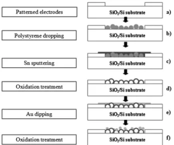
Bar-type sensor electrodes were patterned on SiO
2/Si substrate of 5 mm × 5 mm dimension by the dc sputtering of titanium (30 nm) and platinum (150 nm) in sequence through a metal shadow mask. A PS sphere solution was formed by dispersing 1 wt% PS sphere powder in a mixture of water and ethanol (1:5). A few droplets of the PS sphere solution were dropped onto the patterned substrate, followed by drying at 100
oC for 5min to form a PS spheres array onto the substrate(Fig. 1a and 1b).
The Sn metal was subsequently deposited onto the sub- strate by dc sputtering the Sn target (99.99 % purity) through a shadow mask for 30s, 60s, and 120s(Fig. 1c).
Notably, Sn metal was coated only on the top half of the stacked PS spheres because of the directionality of the sputtered beam and involved shadowing effect. The pre- pared Sn/PS-sphere/SiO
2/Si-substrate was heated in an
air-ambient furnace at 600
oC for 2h to burn out the PS spheres while converting Sn to SnO
2nanocrystallites to form array of hollow SnO
2hemispheres. In the process, SnO
2hollow hemisphere arrays collapsed down on the substrate(Fig. 1d). Consequently, a two-dimensional quasi- periodic SnO
2hollow hemisphere array structure was formed on the SiO
2substrate.
The oxidation temperature was varied at 600, 700, and 800
oC to find the highest response condition of the structure. The SnO
2HA film was also dipped into gold solution followed by oxidation process to study the Au decoration effect on methane sensing. Along with Sn HA structure fabrication, we also fabricated thin film struc- tures via sputter deposition on plane substrates to compare with the performance from the HA sensor structures. The samples were identified by the structure, sputtering time, and oxidation temperature like ‘HA-30-600’ for HA structure of 30s sputtering and 600
oC oxidation.
The surface morphology and structural properties of the sensing films were investigated by field-emission scanning electron microscopy(FE-SEM; JSM 700F; JEOL).
The schematic apparatus for measuring the sensing property is shown in Fig. 2. The gas sensing properties were measured using a pico-ammeter/voltage source (Keithley 6487). We used 1000ppm CH
4gas diluted in nitrogen as the analyte gas. The gas was further diluted in dry air by varying CH
4concentration at a constant dry air flow rate of 300 sccm when fed into the test chamber.
Resistances were measured by applying 1 V bias between the two electrodes while flowing gases into the chamber.
The response of the gas sensor is defined by S = (R
g− R
o)/R
o, where R
oand R
gis the resistance of the sensor structure before and after flowing the methane gas.
3. Results and Discussion
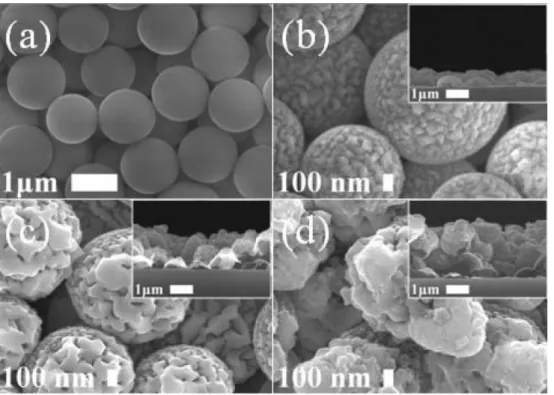
Fig. 3a shows the surface morphology of the synthesized PS sphere array coated onto the substrate. Multiplayers
Fig. 1. Schematic of the fabrication procedure for hollow SnO2 hemi-
sphere array structure for gas sensors. Fig. 2. Schematic diagram of the gas sensing measurement system.
of PS spheres with a uniform size of approximately 1 µm are covered on the substrate. The morphology of Sn HA structures of varying sputtering times(30 s, 1 m, and 2 m) were shown in Fig. 3b to 3d, which reveal that the Sn thickness did not uniformly increase over the hemispheres.
The average hemisphere wall thicknesses increased with sputtering time, but the thickness uniformity varied sig- nificantly over the spheres due to the shadowing effect of the sputtering. It is thicker on the top in the normal sputtering direction. The morphology of SnO
2HAs after burning out of the PS sphere templates was not different from those before the oxidation process. The morphology of SnO
2HA is shown in Fig. 3b-3d with their cross- sectional views as the inserts, which shows the hollow hemisphere morphology.
The response and recovery behavior upon exposure to 200 ppm CH
4diluted in air was measured at different temperatures between 250 and 500
oC. In our previous study of SnO
2films for NO gas sensing, the oxidation of Sn was carried out at 400
oC for optimum sensing per- formance. However, this oxidation temperature was ex- pected unstable during the sensing property measure- ments because the sensing temperature for methane was found high above 400
oC. This rather high working temperature for CH
4may be due to its covalent bonding nature that requires a high temperature for decomposition.
Therefore, Sn was oxidized at above 600
oC for thermal stability of the sensor structure during the sensing of
methane at above 400
oC. Fig. 4a and 4b show the response-recovery curves measured at different tempera- tures for HA-30-600 sample. The sensors exhibited a typical gas-sensing behavior of an n-type semiconductor as shown by the decrease of the base resistance with exposure to CH
4gas. They all showed good stability and repeatability. The response was ever increasing with tem- perature up to 500
oC, which is the maximum tempera- ture of the measurement system. This trend was similarly observed for different wall thicknesses of 1 m and 2 m sputtering times as shown in Fig. 4c. We can conclude the sample of 30s sputtering revealed the highest re- sponse to 200 ppm CH
4gas because the thickness relatively closer to the depletion thickness.
15)We showed that the highest sensing response in nanostructures can be obtained when the dimension of the structure is near the total depletion condition.
15,16)Therefore, more than 1 m sputtering of Sn produced SnO
2hemisphere wall thickness is thicker than the deletion depth at the given operation temperature.
Fig. 4d shows the summary of the baseline resistance
R
oof the sensors sputtered for different times or of
different HA wall thicknesses. As expected the sample of
longer sputtering showed lower resistance. However, in
contrast to the monotonically decreasing temperature de-
pendence of the resistance for semiconductors, it showed
the maximum at 400
oC. This is due to a change in
oxygen adsorption status on the SnO
2surface. The results
Fig. 3. Planar view SEM images of a) PS spheres coated onto the substrate and hollow SnO2 hemisphere array structures; b) HA-30-600, c) HA-60-600, and d) HA-120-600. Inserts show the cross-section views.454 Nguyen Minh Hieu, Nguyen Minh Vuong, Dojin Kim, Byung Il Choi and Myungbae Kim
showed that the electron extraction from the oxide via oxygen ionosorption is the highest at a middle tempera- ture of 400
oC. The density of the adsorbing oxygen on the oxide surface changes increases with temperature up to 400
oC probably due to increasing decomposition rate, but the desorption enhancement effect may be higher at above 400
oC. This observation is very interesting because the operation temperature for the maximum resistance (400
oC) do not coincide with that for the maximum sensing response (500
oC). If one can write the reaction equation on the surface as CH
4+ 4O
−→ CO
2+ 2H
2O + 4e
−, the discrepancy indicates that the reaction rate of CH
4with O
−contributes more to the response level enhancement than the oxygen adsorption density on the surface. In other words, although the density of the adsorbed oxygen ions is decreasing at 500
oC, the in- creasing decomposition rate for CH
4enhanced the over- all gas sensing reaction rate.
The high working temperature of a sensor can be a problem in the sense of stability and safety as well as of the power consumption. Thus reducing the operation temperature is an important issue for methane sensing.
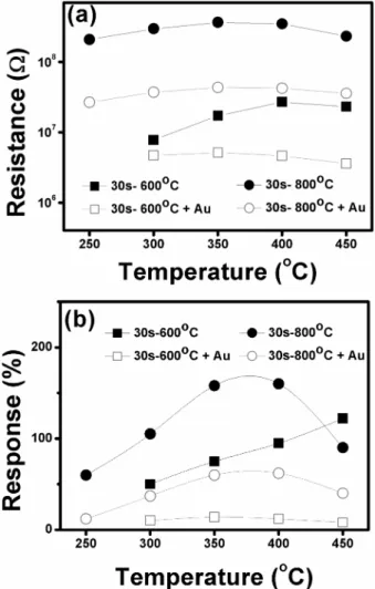
Since the first attempt to change the sensor property is changing the oxidation condition of the material, we tried to increase the oxidation temperature above 600
oC. Fig.
5a shows the response-and-recovery curves of SnO
2HA
structures fabricated from different oxidation tempera- tures(or HA-30-600, HA-30-700, and HA-30-800). They were measured at 400
oC to 200 ppm CH
4. First of all, note that the baseline resistance has increased with oxidation temperature. That was ~3 × 10
7Ω for 600
oC,
~4 × 10
8Ω for 700
oC, and ~1 × 10
9Ω for 800
oC. The higher oxidation temperature could enhance the cry- stallinity of the oxide by removing the oxygen vacancies.
We observed such change in the oxygen deficiency δ(in the notation of SnO
2-δ) along with the oxidation tem- perature change.
17)The observed temperature dependent sensing responses
shown in Fig. 5b are more remarkable. 1) the highest
response of ~220 % was obtained at 400
oC from HA-30-
800 sample and 2) the maximum and optimum working
temperature has decreased to 350-400
oC with high oxi-
dation temperatures. If the higher crystallinity of the
SnO
2produced the higher response, the state of oxygen
adsorption on the highly crystalline surface and related
catalytic effect on the surface gas reaction need to be
invoked. This interpretation is not clear at present and
requires further exploration because defective crystalline
state may show higher catalytic effect. A possible ex-
planation is the doping effect. All the samples have same
thicknesses in average due to the same sputtering time,
and therefore, the different resistances for different
Fig. 4. Sensing properties (a) and their resistance variation (b) of sample HA-30-600 to 200 ppm CH4 gas measured at different operation temperatures. (c) Operation temperature dependence of sensor responses from samples HA-30-600, HA-60-600, and HA-120-600. (d) Tem- perature dependent resistances of the samples in air environment.oxidation temperatures can exhibit the different doping levels. The consequence is the different depth for total depletion due to the semiconductor junction theory, and the samples are at different depletion depth conditions in the air environment. The maximum responses for 700 and 800
oC oxidation cases were then resulted from the total depletion condition of the structures at the inter- mediate working temperatures of 350-400
oC. We experi- mentally and theoretically showed that the nanowire structures at the total depletion condition reveal the maxi- mum sensor response.
15)The maximum response was then observed by chance because the samples HA-30-700 and HA-30-800 were nearly depleted of electrons at the
working temperature. The results so far support the carrier depletion mechanism for the sensing responses with nano-thickness film structures.
A data from a planar thin film structure, TF-30-800, was also illustrated in Fig. 6 for comparison. The base- line resistance was ~6 × 10
6Ω, which is about 200 times lower than the corresponding HA structure. As seen from the resistance value, the thin film structure was not optimized for the high response so that a direct com- parison with the corresponding HA structure is not fair.
Nevertheless, the observed response level is far smaller than the HA sensor having similar resistance value, and this enhancement could be observed from the morphology of floating film so that the analyte gas can approach from
Fig. 5. a) Sensing responses measured at 400oC for 200 ppm CH4gas from the sensors fabricated by oxidation at different tempera- tures(HA-30-600, HA-30-700, and HA-30-800) and b) temperature dependent response values of the sensors.
Fig. 6. a) Sensing responses measured at 400oC for 200 ppm CH4 gas from the sensors of hemisphere array and thin film structures (HA-30-800 and TF-30-800) and b) temperature dependent response values of the sensors.
456 Nguyen Minh Hieu, Nguyen Minh Vuong, Dojin Kim, Byung Il Choi and Myungbae Kim
both surfaces of the films. We also examined gold doping to test the possibility of further working temperature reduction. Two samples, HA-30-600 and HA-30-800, were gold doped for the comparison. Responses of the samples are shown in Fig. 7. Both cases revealed similar trend:
resistances and responses have decreased and working temperature lowering effect was not observed. The lowered response from the lowered resistance sample can be understood again from the un-optimized film resistance.
Therefore, fair comparison of an influence of a parameter on the sensor performance requires setting the resistances at the same level. This issue needs further detail ex- ploration.
4. Conclusions
A low-cost, easy fabrication process for the 2D hollow SnO
2hemisphere array structures for highly responsive CH
4gas sensors was developed by sputtering Sn on arrayed PS spheres followed by oxidation. The sputter-
deposited Sn on top of the PS spheres formed hemi- spheres and collapsed down on the substrate while burning the PS spheres during oxidation. The response we obtained is very impressive in comparison with other reported SnO
2sensors for CH
4gas. This high sensing performance resulted from the nano-size effect or the very thin walls of the grain network. The hemisphere morphology enabled a response of more than an order of magnitude higher than that of a thin-film type SnO
2sensor. This result proved that high porosity in an ensemble of nanostructures and nanostructure geometries open to the exterior facilitated easy access of target gas molecules, thereby leading to high responses. Au addition also added to this study but didn’t express much infor- mation due to lower gas sensitivity in comparison with our initial HA structure.
Acknowledgements
This work was supported by the principal research program of the Korea Institute of Machinery and Materials (KIMM) and the National Research Laboratory program of the National Research Foundation of Korea.
References
1. D. E. Williams, Sens. Actuators, B, 57, 1 (1999).
2. G. X. Wang, J. S. Park, M. S. Park and X. L. Gou, Sens.
Actuators, B, 131, 313(2008).
3. D. Wang, X. F. Chu and M. L. Gong, Sens. Actuators, B, 117, 183 (2006).
4. C. Zheng, Y. Chu, Y. Dong, Y. Zhan and G. Wang, Mater. Lett., 59, 2018(2005).
5. T. Hyodo, S. Abe, Y. Shimizu and M. Egashira, Sens.
Actuators, B, 93, 590 (2003).
6. G. Xi, Y. He, Q. Zhang, H. Xiao, X. Wang and C. Wang, J. Phys. Chem. C, 112, 11645 (2008).
7. R. G. Deshmukh, S. S. Badadhe, M. V. Vaishampayan and I. S. Mulla, Mater. Lett., 62, 4328(2008).
8. J. H. Lee, Sens. Actuators, B, 140, 319 (2009).
9. X. Sun, J. Liu and Y. Li, Chem. Eur. J., 12, 2039 (2006).
10. T. Hyodo, K. Sasahara, Y. Shimizu and M. Egashira, Sens. Actuators, B, 106, 580(2005).
11. J. Zhang, S. Wang, Y. Wang, Y. Wang, B. Zhu, H. Xia,X.
Guo, S. Zhang, W. Huang and S. Wu, Sens. Actuators, B, 135, 610 (2009).
12. Y. Xiao Ming, L. Cheng Chao, Z. Ming, H. Quan Yi, L.
Shuang, L. Qiu Hong, C. Li Bao and W. Tai Hong, Nano- technol., 20, 455503 (2009).
13. L. He, Y. Jia, F. Meng, M. Li and J. Liu, J. Mater. Sci., 44, 4326 (2009).
14. H. N. Hieu, N. M. Vuong, H. Jung, D. M. Jang, D. Kim, H. Kim and S. -K. Hong, J. Mater. Chem., 22, 1127 (2012).
Fig. 7. a) Resistance variation of samples HA-30-600, HA-30-800, HA-30-600-Au, and HA-30-800-Au and b) their response values measured at 400oC for 200 ppm CH4 gas.
15. A. Rothschild and Y. Komem, J. Appl. Phys., 95, 6374 (2004).
16. N. M. Vuong, H. Jung, D. Kim, H. Kim and S. -K.
Hong, J. Mater. Chem., 22, 6716 (2012).
17. N. D. Hoa, N. V. Quy, D. Kim, Sens. Actuators, B, 142, 253 (2009).