<연구논문>
한국표면공학회지
J. Korean Inst. Surf. Eng
ISSN 1225-8024(Print) Vol.54, No.1, 2021.ISSN 2288-8403(Online) https://doi.org/10.5695/JKISE.2021.54.1.18
1. Introduction
(KNN) has been attracting atten- tion as a material that can replace piezoelectric compounds based on lead(Pb) due to high Curie temperature(
=420℃), bioaffinity and high fer- roelectricity, and piezoelectric properties(residual polarization
=33
, piezoelectric co- efficient
=160) [1]. Since compounds such as PZT and PMN, which are based on hav-
ing excellent piezoelectric and ferroelectric prop- erties, are not free from environment problems, the emergence of KNN in the 1950s has attracted attention from many [2-4]. In particular, KNN is used for ferroelectric random access memory, multi-layer ceramic capacitor, superelectric sensor and electric optical device due to its excellent ferroelectric properties [5-8]. According to Saito [9], the preferred (100) direction of KNN grains is considered as the main variable for optimizing the characteristics of KNN materials. The KNN thin films showing the characteristics of the (100) direction of the cubic bodies formed during KNN synthesis can be manufactured variously on Pt, Ti
Manufacture and Surface Structure Characteristics of Mn-Doped Films
Yeon Jung Kim
1· Jaeduk Byun
2· June Won Hyun
2*1
College of Engineering, Dankook University, Yongin 16890, Korea
2
Department of Physics, Dankook University, Cheonan 31116, Korea
(Received 28 January, 2021 ; revised 20 February, 2021 ; accepted 24 February, 2021)
Abstract
KNN is widely used in the electronic industry such as memory devices, sensors, and capacitors due to various structural, electrical, and eco-friendly properties. In this study, Mn-doped KNN was prepared by adopting a sol-gel method with advantages of low cost and large area thin film fabrication. The Mn-doped KNN thin films were deposited by annealing in air for 1 hour and 700° C. The surface morphology characteristics and grain size of the heat-treated KNN were observed by SEM and AFM, and we used the X-ray diffraction for measuring the crystal phase of KNN. The XRD analysis results show that the fabrication of
thin films by sol-gel method in the thin film process of this experiment was stable in the perovskite phase of c-axis orientation. The SEM and AFM results show that the cracks were not confirmed from the fracture surface data of KNN thin films and were densely deposited with thin films with uniform thickness.
Keywords : KNN, Manganese (Mn) ion, Sol-gel, Thin film
*Corresponding Author: June Won Hyun
Department of physics, Dankook University
Tel: +82-41-550-3496 ; Fax: +82-41-559-7858
E-mail: [email protected]
and Si substrates [10]. Especially, various elec- trical characteristics including dielectric properties can be examined by doping materials such as Li, Mg, Ta, and Mn in
. The role of doping materials theoretically and experimentally occupies a very important position in the study of optical, magnetic and electrical properties. In this study, in Mn doping effect of KNN was investigated. The structural characteristics were analyzed by Field emission scanning electron mi- croscopy(FE_SEM, HITACHI, S-4300) and X-ray diffraction(XRD, Rigaku). In order to manufacture KNN thin films, various processes such as RF sputtering method, pulsed-laser deposition meth- od, sol-gel method are used [11,12]. In this study, we have adopted a sol-gel method that is relatively inexpensive and relatively manufactur- ing easy to manufacture and can coat with large area compared to other manufacturing processes.
However, the sol-gel method has a disadvantage in the high heat treatment temperature compared to other processes, and it has been reported that the diffusion of Si on the silicon substrate, which is commonly used during the thin film manu- facturing process, can form a
-like com- pound [13]. Therefore, it is important to minimize the formation and growth of these compounds. In addition, it is important to determine the optimal Mn doping amount to improve the crystallinity of KNN, because the addition of the Mn doping amount leads to a decrease in crystallinity. In this study, we observed the grains with the out-of-plane texture (100) direction due to Mn doping after the Mn-doped KNN thin film was fabricated using sol-gel method.
2. Experiment
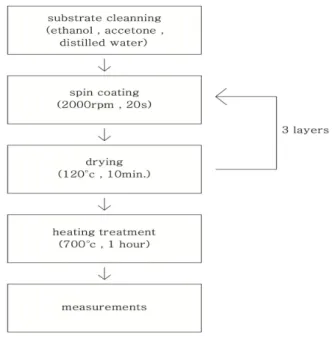
As shown in Figure 1,
(=0.010, 0.005) thin film was fabricated on Si substrate by sol-gel method. To clean the substrate, the surface for- eign substances were removed by ethanol and
acetone, and then finally washed with distilled water. In addition, the substrate was cleaned once more with nitrogen gas to remove a fine amount of pollutants. The KNN sol solution was dropped on the Si substrate which was washed in this way and maintained for 20 seconds at a spin speed of 2000 rpm using spin coater. After spin coating, the substrate was treated at 120℃ and 10 minutes of heat transfer in the oven. The spin coating process was repeated three times to bring about the multi-layered thin film effect. After that, the post-heat treatment was increased to a constant rate of 200℃ per hour for high quality thin film environment, and the temperature envi- ronment was maintained for 1 hour after reaching 700℃. The two thin films formed by depositing and growing crystals by substituting x = 0.005 and x = 0.010 mole% of Mn at the Nb-site of KNN, respectively, were named KNNMn05 and KNNMn10.
The surface of the sample prepared to analyze the surface shape of the specimen was analyzed using Field emission scanning electron micro- scopy(FE-SEM) and Atomic forced micro- scopy(AFM). In addition, the crystallinity of the specimen was confirmed by using X-ray dif-
Fig. 1. Flow chart showing the process for
manufacturing (K
0.5Na
0.5)(Nb
1-xMn
x)O
3thin films.
fraction(XRD). The measurement condition was measured between 20 and 50(2θ) degree of dif- fraction angle using CuK α of λ=1.542Å.
3. Results and discussion
3.1 Analysis of XRD structure
In the previous study, the XRD analysis of fer- roelectric KNN ceramics showed that it was grown by the crystallization of perovskite struc- ture with a dense and uniform structure [14,15].
By substituting Mn,
[KNNMn05] and
[KNNMn10] thin films were deposited to analyze the crystal structure and surface morphology.
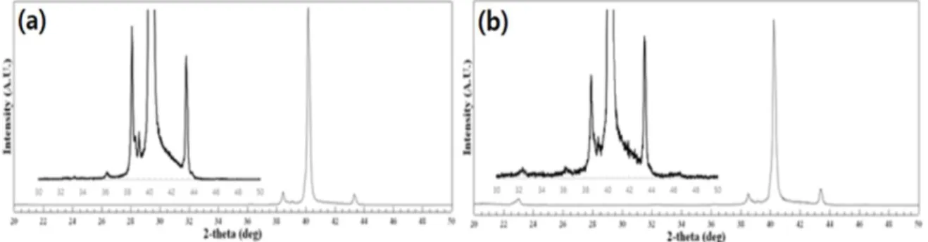
Figure 2 shows the XRD diffraction peaks of KNNMn05 and KNNMn10 thin films in which Mn is substituted with x=0.005 and x=0.010 mole% at the B site of pure perovskite KNN. In the sol sol- ution of the stoichiometric KNNMn05, K was an- alyzed as 50%±0.004, Na was 50%±0.012, Nb was 99.0%±0.020, Mn was 1.0%±0.006, while in KNNMn10, K was analyzed as 50%±0.008, Na was 50%±0.012, Nb was 99.0%±0.020, and Mn was 1.0%±0.002. It was confirmed that the sol solution was stably synthesized. In general, it is very dif- ficult to synthesize group 5 transition metals Nb
5+and alkali metals K
+and Na
+into a KNN thin film due to the difference in chemical properties of these elements. When sol is synthesized, the excess K and Na are added by 10~20 mole% and the sol solution is synthesized so that the gen- eration of the
pyrochlore phase of the tungsten bronze structure obstructing the ferro-
electric property can be suppressed. The ferro- electric thin film on the stable single perovskite can be manufactured. It is not easy to determine the chemical composition of perovskite KNNMn05 and KNNMn10 thin films on
substrate after heat treatment. However, when the raw materials were manufactured, the stoichi- metric sol-gel was stably prepared to deposit KNNMn05 and KNNMn10 thin films. As shown in the Figure 2. the half-width of the diffraction peak on the thin film surface did not change sig- nificantly regardless of the amount of Mn added.
KNNMn05 and KNNMn10 thin films substituted with x=0.005 and x=0.010 mole% were stably crystallized, and as a result, they were grown into pure perovskite thin films. This is because small amounts of Mn can be substituted for KNN to grow relatively stable thin films due to a drop in crystallization temperature and an increase in crystallization density. Typically, a polycrystalline KNN thin film grown on a Pt substrate shows XRD diffraction peaks at 2θ=23
o, 32
o, 46
o, 52
o, 57
oand 67
o[16]. Unlike the non-stoichimetric sol-gel KNN thin films, the KNNMn05 and KNNMn10 thin films deposited by adding Mn for 1 hour at 700° C were not observed to have dif- fraction peaks of the pyrochlore phase
near 33°. The crystallization was achieved on a single perovskite. In addition, as a result of ana- lyzing the XRD data of KNNMn05 and KNNMn10 in Figure 2, it can be seen that the two thin films in which Mn is replaced by x = 0.005 and x = 0.010 mol %, respectively, show strong diffraction peaks in the (200) plane. The pure perovskite KNN thin film is oriented in the direction of the
Fig. 2. XRD patterns of (a) KNNMn05 and (b) KNNMn10 thin films fabricated at 700° C for 1 hour on
Pt/Ti/SiO
2/Si substrates.
(100) substrate, and the (100) diffraction peak is relatively greater than the (200) diffraction peak due to the lowest surface energy of the (100) crystal surface [17]. However, in the case of the sample with 0.005 mole% of Mn in Figure 2(a), the diffraction peak of the (100) surface was not observed clearly, and the sample with 0.010 mole% of Mn in Figure 2(b) was found to have a diffraction peak of (200) near 45~46°. Also, dif- fraction peaks of the (100) surface were observed near 23~24°. The fabrication of
thin films by sol-gel method in this experiment was stable in the per- ovskite crystal of c-axis orientation, and the XRD results are well consistent with the results of the study that KNN single crystals, polycrystals, and thin films grows to have orthorhombic symmetry of other researchers [18-22]. The difficulty of growing KNN thin film of the perovskite
single phase can improve ferroelectricity and pie- zoelectricity by replacing Mn, Li, Ta, La etc. in A and B site of the
crystalline structure.
KNN thin films will be environmental and can be widely used.
3.2 SEM analysis
Figure 3(a, c) is a typical SEM image for ana- lyzing the surface morphology of KNNMn05 and KNNMn10 thin films deposited by annealing in air for 1 hour and 700° C. The two compositions of KNNMn05 and KNNMn10 were crystallized in any direction on
substrates and formed a perovskite single phase. The chemical component of pure KNN thin films was analyzed by EPMA, and the ratio of
was 0.86%±0.04 and was the smaller than 1.0. This means that when the amount of alkali metal is over-added by 10%,
and
are relatively volatile during the heat treatment process [23].
The KNN thin film was known to exhibit better dielectric and piezoelectric properties than other lead-free ferroelectric thin films, but the sol sol- ution of this experiment was synthesized by add-
ing Mn. KNN thin films have great difficulties depending on the atomic arrangements required for composition control and piezoelectric effect. In other words, since the atomic arrangement con- ditions required for piezoelectric effects depend very sensitively on chemical composition, it is very difficult to obtain excellent piezoelectric properties by stably fabricating thin films based on KNN system. Therefore, it is important to suppress the loss of volatile factors required for stable synthesis conditions KNN system. Of course, it is relatively difficult to grow the ferro- electric KNN thin films which can be applied by over-adding
and
to be compact and stable, but it can be grown into a stable BO
6per- ovskite structure by replacing the K, Na, and Nb sites of KNN with other elements such as Ag, La, Li, Ta, and Mn. By controlling well the interaction between the volatile K within the sol solution, and the Na alkali ion and stabilizer, the volatile of K, and Na are suppressed and the composition of the thin film is kept steadily. In this way, it is possible to lower the crystallization temperature by substituting the A and B sites of the ABO
3perovskite structure KNN. The fracture surface of KNNMn05 and KNNMn10 thin films after heat treatment for 1 hour and 700° C in air by adding Mn of Figure 3(b, d) showed that crack was not confirmed and it was densely deposited with thin films with uniform thickness. The average grain size of KNNMn05 and KNNMn10 thin films was 149 nm and 154 nm, respectively. However, there was no significant difference in the average grain size in KNNMn10, where the substitution amount of Mn increased to 0.010 mole% in KNNMn05, where the substitution amount of Mn was 0.005 mole%, but the grain size of KNNMn10 thin film treated after heat treatment for 1 hour and 700°
C in air was slightly larger than the grain size of
KNNMn05. It indicates that it has grown
continuously. On the other hand, the formation of
grains mixed with spherical and columnar struc-
tures in KNNMn05 and KNNMn10 thin films is
analyzed by the formation of pyrochlore phases in
a small unit area due to rapid volatilization of al- kali ions as analyzed by XRD results. In Figure 3(b, d), the deposition thickness of KNNMn05 and KNNMn10 thin films were measured at 412 nm and 423 nm, respectively. The partial cracks shown in Figure 3(a, c) are caused by residual strain on the surface of the thin film, which causes a change in the crystal structure per unit volume of the thin films due to the thermal ex- pansion of the Pt substrate and repeated pyrolysis of the deposition layer in the spin coating process 1 to 3 times [24].
3.3 Analysis of AFM
Figure 4(a, b) is a typical AFM image for the surface roughness analysis of KNNMn05 and KNNMn10 thin films. We compared the SEM analysis data of KNNMn05 and KNNMn10 thin films, and determined the RMS roughness of the thin films by AFM analysis of the surface mor- phology and topography. The surface roughness was obtained in the scan range of 5 um x 5 um thin film, and it was confirmed that all deposited
thin films grew into nano polycrystals of about ~15 nm. The rough- ness of the surface of the KNNMn10 thin film, which substituted 0.010 mole% of Figure 4(b), was significantly increased compared to the KNNMn05 composition, which substituted 0.005 mole% of Mn of Figure 4(a). In other words, the increase in the substitution of Mn increases the surface roughness as well as the surface mor- phology, and the particle size increases sig- nificantly according to the amount of excess al-
kali ions. In addition, the size of the grains in- creased slightly with the increase of the concen- tration of the sol solution. However, several re- searchers reported that the surface roughness of pure KNN thin films does not depend heavily on crystallization temperature [25]. The RMS rough- ness of KNNMn05 polycrystalline thin films sub- stituted for Mn was 15.04 nm, and the RMS roughness of KNNMn10 thin films substituted for Mn with 0.010 mole% was observed to be 8.48 nm. This is consistent with the analysis results of the surface state of SEM images in Figure 3(a, b) well, and the size of grains of Mn-doped
thin films is related to the formation of vacancies due to the chemical bonding of cations and anions during the crystal- lization of thin films by heating treatment. In ad- dition, it was analyzed that the addition of Mn has a significant influence on the nucleation and crystal growth processes of the KNNMn05 and KNNMn10 thin films. This result is generally due to the relatively easy process of alkali ion defects due to active volatilization of alkali ions and ex- cessive oxygen deficiency during the pyrolysis of KNN thin films [21, 26]. Thus, the introduction of
can absorb this
(hole) by increasing the valence of
, which is represented by
+
→
,
+
→
. Therefore,
the chemical composition of
deposition solution
should be controlled precisely, unlike pure KNN
thin films, since the ferroelectric properties can
be improved by significantly reducing oxygen de-
Fig. 3. SEM images of (a, c) KNNMn05 and (b, d) KNNMn10 thin films fabricated at 700° C for 1 hour on
Pt/Ti/SiO
2/Si substrates.
ficiency and hole of
thin films substituted with Mn on KNN thin films.
Fig. 4. AFM images of (a, c) KNNMn05 and (b, d) KNNMn10 thin films fabricated at 700° C for 1 hour on Pt/Ti/SiO
2/Si substrates.
4. Conclusions
This study analyzed the fabrication conditions of environment-friendly lead-free ferroelectric
thin films with ex- cellent ferroelectricity and used a sol-gel method to improve stably ferroelectric and piezoelectric properties of
and