1. INTRODUCTION
Direct engineering of a graphene field-effect transistor (FET) provides high-precision control of its electronic/
electrical properties to design a multifunctional, unique device platform which can be utilized in a variety of applications including electronics, computing, sensors, and so [1-5]. A simple graphene FET device structure is divided into two parts, channel and contact areas [3,6].
Modification of the channel area of graphene involves functionalization or doping, which prepares active sites for detecting target species to develop high-performance sensors or which possibly opens up an electronic bandgap of graphene for a high on/off ratio FET transistor as well as to design graphene-based spin electronics for quantum computing applications [1,5,7,8]. Contact engineering is to
✉ Songkil Kim; [email protected] Copyright ©2020 KIEEME. All rights reserved.
This is an Open-Access article distributed under the terms of the Creative Commons Attribution Non-Commercial License (http://creativecommons.org/licenses/by-nc/3.0) which permits unrestricted non-commercial use, distribution, and reproduction in any medium, provided the original work is properly cited.
tune heterogeneous graphene-metal interfacial properties having intrinsically poor electrical and mechanical robustness which is the continuing challenge in graphene electronics [3,6]. Compared to weak coupling through con- ventional metal contact fabrication, additional treatments were verified to induce strong chemical binding for improved interfacial properties of graphene-metal, finally leading to non-trivial enhancement of the device performance [3,6,9].
Focused electron beam induced processing (FEBIP) is a resist-free nanolithographic technique enabling nano- fabrication in a multi-mode format including geometrical patterning, functionalization/defect formation and doping as well as metal and metal oxide deposition, based on electron-matter interaction [1-3,5,10]. The FEBIP uses a tightly focused electron beam and is implemented in an electron microscopy environment, allowing for high- resolution nanofabrication with in-situ imaging of nano- materials and structures at atomic-to-micro scales [10-16].
Depending on a diameter of a focused electron beam, the resolution of the process can be determined with various imaging resolutions under different electron mi- croscopy environments. Scanning transmission electron microscope
Focused Electron Beam-Controlled Graphene Field-Effect Transistor
Songkil Kim
School of Mechanical Engineering, Pusan National University, Busan 46241, Korea
(Received July 27, 2020; Revised August 11, 2020; Accepted August 12, 2020)
Abstract: Focused electron beams with high energy acceleration are versatile probes. Focused electron beams can be used for high-resolution imaging and multi-mode nanofabrication, in combination with, molecular precursor delivery, in an electron microscopy environment. A high degree of control with atomic-to-microscale resolution, a focused electron beam allows for precise engineering of a graphene-based field-effect transistor (FET). In this study, the effect of electron irradiation on a graphene FET was systematically investigated. A separate evaluation of the electron beam induced transport properties at the graphene channel and the graphene-metal contacts was conducted. This provided on-demand strategies for tuning transfer characteristics of graphene FETs by focused electron beam irradiation.
Keywords: Focused electron beam induced processing (FEBIP), Graphene, Graphene field-effect transistor
DOI: https://doi.org/10.4313/JKEM.2020.33.5.360
ISSN 1226-7945(Print), 2288-3258(Online)
(STEM) uses a focused electron beam as a probe whose diameter is ~0.1 nm, enabling atomically-resolved imaging of materials and atomic manipulation of nanomaterials [13,14]. Local interaction of electrons with solid state materials has been extensively studied to demonstrate atom-by-atom fabrication of 2D nanomaterials, as termed as atomic forge [17,18]. For a larger scale fabrication of 2D nanomaterials, scanning electron microscope (SEM) was utilized. It enables nano-to-microscale manipulation of 2D nanomaterials using a focused electron beam with a diameter of ~3 nm or larger at an accelerating voltages from few hundreds eV to 30 keV [1-3,5,11,12]. The FEBIP in a SEM environment allows for a large area patterning and fabrication of operational devices in combination with the directed flow of molecular pre- cursors to electron beam irradiation sites in the SEM chamber through a gas injection nozzle installed to the SEM.
The FEBIP was applied to graphene-based FET devices for engineering device performances and functionalities.
As the perspectives of material design, graphene channel regions were functionalized with hydrogen or fluorine atoms to modulate functional properties of graphene, for example, engineering an electronic bandgap and enhancing magnetic properties [1,2,5]. In addition, recent studies de- monstrated that controlling an electron irradiation dose can modify the doping state of graphene; low electron dose induces n-p-n type doping with the localized formation of carbon near the contact areas, while a high electron dose can lead to n-type doping with the coverage of carbon over the entire channel area [19,20]. Also, the well-controlled electron irradiation at graphene-metal contacts can generate localized defects and induce the transformation of detrimental, interfacial polymer residues into graphitic interlayer, which enhances interfacial properties of the graphene-metal contacts and increase the device performance [3]. Even though the systematic studies have been conducted to understand the mechanism about electron beam induced engineering of graphene FET device performances, no separate evaluation of contact and channel transport properties in a graphene FET device after electron beam irradiation has been implemented. In this study, a graphene field-effect transistor was fabricated and the effect of electron beam irradiation on a graphene
FET device was systematically investigated with an emphasis on the separate evaluation of electrical transport properties at the channel and the graphene-metal contacts.
2. EXPERIMENTAL METHODS 2.1 Graphene transfer
A large scale monolayer graphene film was grown on a copper foil using a low pressure chemical vapor deposition (LPCVD), and graphene was transferred onto a SiO
2/Si substrate (1 cm × 1 cm) using a wet transfer method [20]. A wet transfer method involves a spin coating of poly methyl methacrylate (PMMA) as a supporting film on top of graphene/copper foil, which was followed by etching the copper foil by floating PMMA/graphene/copper foil on a ammonium persulfate/
DI water etching solution. Then, the PMMA/graphene was scooped by the SiO
2/Si substrate. The sample was heated at 150℃ on a hot plate to achieve a better adhesion of PMMA/graphene to the substrate. The PMMA layer was then removed by soaking the sample in an acetone at 80℃ to terminate the graphene transfer.
2.2 Device fabrication
The transferred graphene film was spin-coated with PMMA resist and e-beam lithographically patterned for defining a 1.3 μm (width) × 60 μm (length) graphene strip, followed by oxygen plasma reactive ion etching (RIE) of graphene to fabricate the conductive channel for the graphene FETs. Then, the source/drain metal electrodes were lithographically patterned on top of the graphene channel with deposition of 10 nm Cr/30 nm Au, followed by lift-off of PMMA resist in a heated acetone bath at 80℃.
2.3 Electron irradiation
Electron irradiation was conducted using a focused
electron beam at an accelerating voltage of 25 keV and a
beam current of ~400 pA in a scanning electron microscopy
(FEI Quanta 200) maintained at ~10
-6Torr. The electron
beam irradiation was controlled using nanometer pattern generation system (NPGS) software. The electron irradiation dose was varied by changing a beam dwell time at a spot over the same irradiation area of 400 nm × 400 nm on graphene-metal contacts.
2.4 Characterization
Topography images were obtained using a Dimension- 3,000 atomic force microscope with a silicon tip in a tapping mode. Raman measurements of graphene before/
after electron irradiation were carried out using a WITec (Alpha 300 R) confocal Raman microscope with 514.5 nm excitation wavelength of an Ar
+ion laser.
3. RESULTS AND DISCUSSION
The inset of Fig. 1(a) shows the optical microscopy image of the fabricated device. The graphene channel
has its length of 5 μm with a width of 7 μm, and the metal contact width on top of the graphene channel is 1 μm. The transfer curve of a graphene FET is shown in Fig. 1(a), exhibiting source-drain currents (I
ds) measured by sweeping a back-gate voltage (V
bg) from -35 V to 40 V at different source-drain voltages (V
ds). An average current on/off ratio was measured as 2.93±0.5 and the device s hows the p-doping state with a Dirac voltage shift to ~11.4 V which is due to polymer residues on the graphene channel as a result of device fabrication process [20,21]. Figure 1(b) shows an atomic force mi- croscopy (AFM) surface topography image of the graphene channel measured in a tapping mode using a silicon tip which confirms the presence of the polymer residues on graphene surface.
After mild electron irradiation on the metal contact area of the graphene device at an electron dose of 4.5×10
18electrons/cm
2, the transfer curve of the graphene
(a)
(b)
Fig. 1. (a) The electrical transfer curve (Ids-Vbg) of an as-fabricated graphene FET with the inset showing the optical microscope image of the device and (b) the AFM surface topography image of the graphene channel showing the presence of the polymer residues (PMMA used as an e-beam resist) as a source for p-type doping of the graphene channel.
(a)
(b)
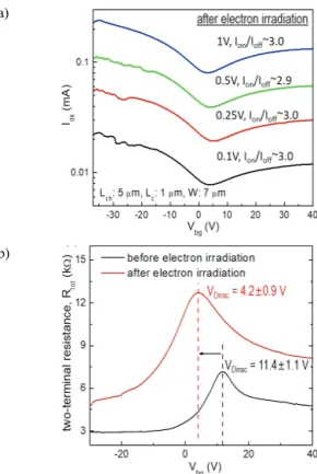
Fig. 2. (a) The transfer curve of the graphene FET after electron irradiation at the graphene-metal contacts with a dose of 4.5×10¹⁸ electrons/cm2 at the beam energy of 25 keV, and (b) the comparison of two-terminal resistances before vs. after electron irradiation depending on a back-gate voltage (Vbg).
device in Fig. 2(a) shows the reduced source-drain currents, but the current on/off ratio maintains similarly as 2.98±
0.05. The change of two-terminal resistances on sweeping a back-gate voltage before and after electron irradiation is shown in Fig. 2(b). Figure 2(b) clearly demonstrates the effect of electron irradiation on the transfer characteristics of the graphene device. The electron irradiation increased two-terminal resistances as much as 77% at a Dirac point (maximum resistance) and 67% of a minimum resistance, but the Dirac voltage was shifted from 11.4 V to 4.2 V, indicating the change of the doping state. The increased two-terminal resistance is due to the combinatorial effect of defect formation on graphene at the metal contact area directly exposed to high-energy (25 keV) primary electrons and the increased carrier scattering sites with carbon deposition on the channel from the source of PMMA residues by secondary electrons (SEs) generated from backscattered electrons. The change of the doping state resulted from the local n-type doping with thin carbon deposits converted from PMMA residues which was the origin of p-type doping on the graphene channel.
Raman spectroscopic measurements of graphene before and after electron irradiation confirmed the change of the doping state, as shown in Fig. 3. The inset of Fig.
3 shows the AFM topography image of the graphene channel with carbon deposition after electron irradiation at the graphene-metal contacts. The AFM image shows the deposited carbon with a thickness of 2~4 nm. The G- and 2D-band peaks were shifted from 1592.4±0.12 cm
-1to 1589.9±0.1 cm
-1and from 2699.4±0.1 cm
-1to 2698.5±0.2 cm
-1, respectively, after carbon deposition by electron irradiation. The red-shifts and broadening of G- and 2D- band peaks indicate the change of the doping state towards n-type doping [22], which is well-correlated with the electrical measurement results showing the shift of the Dirac voltage in Fig. 2(b). The AFM and Raman measurements in conjunction with the electrical measure- ments clearly demonstrate that electron beam induced carbon deposition can lead to the n-type doping of graphene.
To provide the better understanding about the effect of carbon deposition on the channel vs. defect formation at the contacts by the controlled electron beam irradiation on two-terminal transfer characteristic of a graphene FET, separate evaluation of channel and contact resistances was
conducted at different back-gate voltages using a trans- mission line method. The transmission line method (TLM) allows for extracting contact and channel resistances by plotting two-terminal device resistances with the increased length of the graphene channels at the same contact geometry [6]. Figures 4 shows the SEM image of a graphene device structure for the TLM measurements.
Six different channels are denoted in Fig. 4. The graphene- metal contacts were first irradiated over a square area of 400 nm × 400 nm by focused electron beam at the energy of 25 keV during a total irradiation time of 0.64s, which corresponds to the dose of 10
18electrons/cm
2. After the first electron beam irradiation, the TLM device was
Fig. 3. The Raman spectra of the graphene channel before and after electron irradiation. Electron irradiation resulted in the deposition of carbon on the channel area, leading to the red- shift of the representative Raman peaks (G- and 2D-band peaks).The inset shows the AFM surface topography image of the graphene channel after carbon deposition.
Fig. 4. The SEM image of the graphene FET devices for transmission line method (TLM) measurements of contact and channel resistances, showing six channels.
left in an atmospheric condition for 10 days and the 2
ndelectron beam irradiation with a higher electron dose of 10
19electrons/cm
2was conducted at the graphene-metal contacts by the same method done for the 1
stirradiation.
Transfer characteristic (I
ds-V
bg) for each graphene channel was measured by sweeping a back-gate voltage from -40 V to 40 V at a fixed source-drain voltage (V
ds) of 0.1 V. Since the graphene device shows an Ohmic behavior having a linear relation between the source-drain current and voltage at various back-gate voltages, two-terminal resistances were simply calculated by dividing the fixed source-drain voltage with the measured current at selected back-gate voltages. Figures 5(a) and 5(b) show the TLM measurement results at V
bg-V
Diracof 0 V and -35 V before and after the 1
stelectron irradiation, respectively. By linear fitting of the plots [6], we can extract the channel resistance (R
ch) with a slope and the contact resistance (R
c) with a y-intercept, following the relation, R
tot=R
ch+2R
c=(R
sh/W)L
ch+2R
c, where a sheet resistance is defined as R
sh=R
chW/L
chand the width (W) of the graphene channel is ~1.3 µm. The TLM measurement results have a goodness of linear fitting (R
2) near unity, which represents how reliable the TLM measurement results are and indirectly indicates a uni- formity of both the channel and contact properties over the entire set of devices involved in the TLM measurements at the same carrier density.
The extracted sheet and contact resistances upon various V
bg-V
Diracare plotted in Figs. 6(a) and 6(b), respectively. Electron irradiation at the contact areas with a low electron dose can lead to the partial carbon deposition on the graphene channel near the metal contacts and make n-p-n doping on graphene whose electrical resistance in a transfer curve has a secondary peak at a negative V
bg-V
Dirac. The 1
stelectron beam irradiation with the low electron dose formed a n-p-n doping on the graphene channel whose sheet resistance shows the secondary peak near V
bg-V
Dirac=-10 V in Fig.
6(a). Except for the appearance of the secondary peak, the transfer curve of the sheet resistance after the 1
stelectron irradiation is almost similar to that of the devices before electron irradiation, and after 10 days, the transfer curve became almost the same to that before irradiation which is due to the redistribution of
weakly-bound carbon atoms over the graphene channel by surface diffusion. The transfer curve of the contact resistance has a more prominent secondary peak relative to a primary peak and the contact resistance was increased over the entire range of V
bg-V
Dirac. The secondary peak in two-terminal transfer curve with a low electron dose irradiation is mainly due to the carrier transport at the contact. The contact resistance is determined by carrier transports from the metal electrode to graphene or vice versa as well as from the contact to the graphene channel. The overall increase of the contact resistance is due to the defect formation on graphene at the contact region and the presence of the secondary peak results from the different doping states between the contact area and the channel area. After 10 days later, the secondary peaks in both the sheet and contact resistances disappeared which indicates that the redistribution of carbon atoms
(a)(b)
Fig. 5. Transmission line method (TLM) measurement results of the graphene FET devices to extract channel and contact resistances depending on a back-gate voltage: the linear fitting of the measurements for the devices (a) before and (b) after the 1st electron irradiation with a dose of 1018 electrons/cm2, showing a goodness of linear fitting (R2) near unity.
occurred over the entire graphene strip, while the contact resistance still remained higher than that before electron beam irradiation, confirming that the defect formation increased the contact resistance.
After electron beam irradiation at a higher dose of 10
19electrons/cm
2, both sheet and contact resistances increased, but the increase of the contact resistance was far more significant than that of the sheet resistance. It is because the higher electron dose irradiation resulted in the higher density of defects, mostly sp
3-type defects, generated by being exposed to high-energy (25 keV) primary electrons. The shift of the Dirac voltage after the higher electron dose irradiation occurred from 5.1 V (before electron irradiation) to -5.2 V and from 6.7 V to 1.6 V for the shortest channel 1 (channel length of 4.3 µm) and the longest channel 6 (channel length of 32 µm), respectively. With the high electron irradiation dose, the graphene channels were fully covered by the
carbon deposition leading to the change of the doping state towards n-type doping with no secondary peak (no presence of n-p-n doping), but the finite amount of carbon deposition resulted in the difference in the Dirac voltage shift depending on the channel lengths; a short channel will have a higher areal density of carbon, while a long channel will have a lower areal density of carbon.
4. CONCLUSION
In conclusion, we systematically investigated the effect of focused electron beam irradiation at the graphene- metal contact regions on the transfer characteristics of the graphene-based FETs (contact resistance vs. channel resistance). Raman measurements along with AFM surface topography imaging confirmed that electron beam-induced carbon deposition is the origin of the controlled doping state on the graphene devices, whose transfer curves verify the change of the doping state towards n-p-n type doping or n-type doping depending on electron irradiation dose.
Comprehensive understanding about the effect of electron beam irradiation on the graphene FET devices were achieved by separately evaluating sheet and contact resistances from the two-terminal electrical measurement results using the transmission line method. It was found that defect formation by direct irradiation of 25 keV primary electrons at the graphene-metal contact dominates the two-terminal transport curve of the graphene FET than the increased carrier scattering sites by carbon deposited on the graphene channel by low-energy secondary electrons. It is worth noting that our previous study revealed that defect formation at the graphene-metal interface could help enhance electrical conductivity as well as thermo-mechanical properties at the contacts after appropriate thermal annealing to graphitize interfacial carbon deposits, but thermal annealing resulted in significant p-type doping of graphene devices. Overall, this study suggests on-demand strategies for tuning transfer characteristic of graphene FETs by controlled electron beam irradiation; for controlling the doping state, weakly bound carbon deposition can be done selectively on graphene channel with avoiding any exposure to graphene-metal contact regions, but direct irradiation of primary electrons at graphene-metal contacts followed by thermal annealing
(a)(b)
Fig. 6. Transmission line method (TLM) measurement results of the graphene FET devices to extract channel and contact resistances depending on a back-gate voltage: the change of (a) the channel (sheet) resistance and (b) the contact resistance extracted through the linear fitting at various back-gate voltages.
can be a useful strategy to fabricate a highly conductive graphene device for the applications such as graphene- based interconnects.
ORCID
Songkil Kim https://orcid.org/0000-0003-0856-9982
ACKNOWLEDGEMENT
This work was supported by a 2-Year Research Grant of Pusan National University.
REFERENCES
[1] J. Balakrishnan, G.K.W. Koon, M. Jaiswal, A.H.C. Neto, and B. Özyilmaz, Nat. Phys., 9, 284 (2013). [DOI: https://doi.org/
10.1038/nphys2576]
[2] J. D. Jones, K. K. Mahajan, W. H. Williams, P. A. Ecton, Y.
Mo, and J. M. Perez, Carbon, 48, 2335 (2010). [DOI: https://
doi.org/10.1016/j.carbon.2010.03.010]
[3] S. Kim, M . Russell, D. D. Kulkarni, M . Henry, S. Kim, R.
R. Naik, A. A. Voevodin, S. S. Jang, V. V. Tsukruk, and A.
G. Fedorov, ACS Nano, 10, 1042 (2016). [DOI: https://doi.org/
10.1021/acsnano.5b06342]
[4] K. S. Novoselov, A. K. Geim, S. V. Morozov, D. Jiang, Y.
Zhang, S. V. Dubonos, I. V. Grigorieva, and A. A. Firsov, Science, 306, 666 (2004). [DOI: https://doi.org/10.1126/science.
1102896]
[5] F. Withers, T. H. Bointon, M. Dubois, S. Russo, and M. F.
Craciun, Nano Lett., 11, 3912 (2011). [DOI: https://doi.org/
10.1021/nl2020697]
[6] J. T. Smith, A. D. Franklin, D. B. Farmer, and C. D.
Dimitrakopoulos, ACS Nano, 7, 3661 (2013). [DOI: https://
doi.org/10.1021/nn400671z]
[7] B. Cai, L. Huang, H. Zhang, Z. Sun, Z. Zhang, and G. J.
Zhang, Biosens. Bioelectron., 74, 329 (2015). [DOI: https://
doi.org/10.1016/j.bios.2015.06.068]
[8] P. Jangid, D. Pathan, and A. Kottantharayil, Carbon, 132, 65 (2018). [DOI: https://doi.org/10.1016/j.carbon.2018.02.030]
[9] L. Wang, I. Meric, P. Y. Huang, Q. Gao, Y. Gao, H. Tran, T.
Taniguchi, K. Watanabe, L. M. Campos, D. A. Muller, J. Guo, P. Kim, J. Hone, K. L. Shepard, and C. R. Dean, Science, 342, 614 (2013). [DOI: https://doi.org/10.1126/science.1244358]
[10] S. J. Randolph, J. D. Fowlkes, and P. D. Rack, Crit. Rev.
Solid State Mater. Sci., 31, 55 (2006). [DOI: https://doi.org/
10.1080/10408430600930438]
[11] F. J. Urbanos, A. Black, R. Bernardo-Gavito, A. L. Vázquez de Parga, R. Miranda, and D. Granados, Nanoscale, 11, 11152 (2019). [DOI: https://doi.org/10.1039/C9NR02464F]
[12] D. S. Fox, P. Maguire, Y. Zhou, C. Rodenburg, A. O’Neill1, J. N. Coleman, and H. Zhang, Nanotechnology, 27, 195302 (2016). [DOI: https://doi.org/10.1088/0957-4484/27/19/195302]
[13] O. Dyck, S. Kim, E. Jimenez-Izal, A. N. Alexandrova, S.
V. Kalinin, and S. Jesse, Small, 14, 1801771 (2018). [DOI:
https://doi.org/10.1002/smll.201801771]
[14] O. Dyck, S. Kim, S. V. Kalinin, and S. Jesse, Appl. Phys.
Lett., 111, 113104 (2017). [DOI: https://doi.org/10.1063/1.
4998599]
[15] M. Huth, F. Porrati, C. Schwalb, M. Winhold, R. Sachser, M.
Dukic, J. Adams, and G. Fantner, Beilstein J. Nanotechnol., 3, 597 (2012). [DOI: https://doi.org/10.3762/bjnano.3.70]
[16] W. F. van Dorp, B. van Someren, C. W. Hagen, P. Kruit, and P. A. Crozier, Nano Lett., 5, 1303 (2005). [DOI: https://
doi.org/10.1021/nl050522i]
[17] O. Dyck, S. Jesse, and S. V. Kalinin, MRS Bull., 44, 669 (2019). [DOI: https://doi.org/10.1557/mrs.2019.211]
[18] S. V. Kalinin, A. Borisevich, and S. Jesse, Nature, 539, 485 (2016). [DOI: https://doi.org/10.1038/539485a]
[19] Y. Zhou, J. Jadwiszczak, D. Keane, Y. Chen, D. Yu, and H. Zhang, Nanoscale, 9, 8657 (2017). [DOI: https://doi.org/
10.1039/C7NR03446F]
[20] S. Kim, M. Russell, M. Henry, S. S. Kim, R. R. Naik, A.
A. Voevodin, S. S. Jang, V. V. Tsukruk, and A. G. Fedorov, Nanoscale, 7, 14946 (2015). [DOI: https://doi.org/10.1039/
C5NR04063A]
[21] A. Pirkle, J. Chan, A. Venugopal, D. Hinojos, C. W.
Magnuson, S. McDonnell, L. Colombo, E. M. Vogel, R. S.
Ruoff, and R. M . Wallace, Appl. Phys. Lett., 99, 122108 (2011). [DOI: https://doi.org/10.1063/1.3643444]
[22] A. Das, S. Pisana, B. Chakraborty, S. Piscanec, S. K. Saha, U. V. Waghmare, K. S. Novoselov, H. R. Krishnamurthy, A.
K. Geim, A. C. Ferrari, and A. K. Sood, Nat. Nanotechnol., 3, 210 (2008). [DOI: https://doi.org/10.1038/nnano.2008.67]