Development of Wafer Bond Integrity Inspection System Based on Laser Transmittance
Dong-Young Jang1, Hyo-Sok Ahn2, Sajadieh.S.M.Mehdi3,†, Young-Hwan Lim3 and Seok-Kee Hong3
1Departemant of Industrial and Information Systems Engineering, Seoul National University of Technology, 172 Gongreung 2-dong, Nowon-gu, Seoul 139-743, Korea
2Graduate School of NID Fusion Technology, Seoul National University of Technology, 172 Gongreung 2-dong, Nowon-gu, Seoul 139-743, Korea
3Seoul TechnoPark, 172 Gongreung 2-dong, Nowon-gu, Seoul 139-743, Korea (Received March 15, 2010: Accepted June 11, 2010)
Abstract:Among several critical topics in semiconductor fabrication technology, particles in addition to bonded surface contaminations are issues of great concerns. This study reports the development of a system which inspects wafer bond integrity by analyzing laser beam transmittance deviations and the variations of the intensity caused by the defect thickness.
Since the speckling phenomenon exists inherently as long as the laser is used as an optical source and it degrades the inspection accuracy, speckle contrast is another obstacle to be conquered in this system. Consequently speckle contrast reduction methods were reviewed and among the all remedies have been established in the past 30 years the most adaptable solution for inline inspection system is applied. Simulation and subsequently design of experiments has been utilized to discover the best solution to improve irradiance distribution and detection accuracy. Comparison between simulation and experimental results has been done and it confirms an outstanding detection accuracy achievement. Bonded wafer inspection system has been developed and it is ready to be implemented in FAB in the near future.
Keywords:Bonding wafer inspection, Optimization, Simulation, Speckle reduction
1. Introduction
In the world of electronic industries, the performance of electronic products and related accessories could be determined by the performance of semiconductor components. Recently, modern semiconductor packaging technology is one of the most noteworthy technologies to improve the performance of semiconductor parts. Indeed a good number of research efforts are underway for increasing the density of semiconductor devices, and one of the key technologies being developed, is the wafer stack technology, in which silicon wafers are bonded vertically.1)
Wafer bonding, in essence, is a fundamental technology for fabrication of 3D structures in both MEMS and semiconductor fields. However, looming of particles or any air gap on the wafers, referred to as bubbles and voids, points to some un-bonded areas between the wafers resulting in failure of semiconductor devices action.
Therefore, exact methods and sensitive equipments are required to analyze the bonded surface of the bonded wafer effectively.2) In this regard, destructive and non-destructive detections are two categories for the inspection and classification of the defects.
To evaluate the bonded wafer, there are some non- destructive types of equipment at commercial level. They could be categorized based on the method they apply to inspect the defects. Ultrasound inspection and X-Ray inspection are most common technologies capable of analyzing the bonded wafer. However, these methods have some undesirable drawbacks.3) In contrast, laser beam transmission is an appropriate alternative even only laser with wavelength higher than 1000 nm can transmit the silicon wafer.4, 5, 6)
In this study, simulation has been performed by optical design software followed by DOE (Design of Experiments;
Statistical Analysis), which were applied to all gathered data from screening. It delivers the optimized design for the system utilizing laser beam transmission to analyze transmittance deviations and the changes of the intensity caused by the defect thickness.
2. Inspection System concept
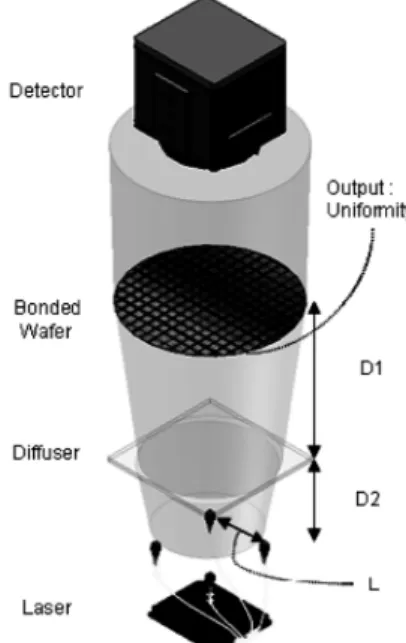
This system, as illustrated in Fig. 1, consists of laser collimators, diffuser sheet, and detector. In this system, fiber type 1064 nm laser is applied. To make it feasible to inspect
†Corresponding author E-mail: [email protected]
almost all area of the bonded surface simultaneously, beam splitter (1×4) has been radiated while four collimators are used. Inevitably, a diffusing plate is used to meet the required uniformity.
3. Simulation
Optical design software has been used in which Monte- Carlo (MC) simulation was applied. In general, the purpose of a simulation is running the models and understanding the results. To do so, it is necessary to plan ahead before doing the runs.7) At first the purpose of simulation is defined and then the real system is modeled in the software phase properly. Factor setting is the next step to be declared.
3.1. Uniformity (Irradiance Standard Deviation) The overall purpose of this study is to find the optimized case to inspect all area of the bonded surface simultaneously.
Moreover, the uniformity of laser spot on inspected area is of critical significance for detecting defects. In this study, standard deviation of irradiance distribution on bonded area has been decided as uniformity. The equation below is applied as
standard deviation formula; where
X and n stands for irradiance and number of simulation output data respectively.8)
3.2. Modeling
Laser source modeling, as the first step of simulation, is done using scattering data produced by experiment. Power of laser is defined as 1W (1×4 splitter) and since only laser with higher wavelength than 1000 nm can transmit the silicon wafer, the wavelength is 1064 nm.
Several runs were done and results ensured that the modeled laser source is equivalent of the laser diode.
Subsequently, three types of diffuser sheets were modeled, with same structure. The structure of diffuser sheet is shown in Fig. 2.
However diffusers modeled with different characteristics,
as described in Table 1, to recognize which parameter has more influence on the irradiance distribution. 8 inches diameter bonded wafer is modeled to be used in simulation as bonded wafer. The thickness of the bottom Silicon layer, Oxide layer and top Silicon layer are 600µm, 10µm and 500µm respectively.
3.3. Factor Setting
It is helpful to assume the simulation as a function that transforms inputs into outputs and of course the functions represent the simulation model itself. It is often of interest to estimate how a change in an input factor affects an output performance measure, i.e. how sensitive an output is to a change in an input.7)
In bonded wafer inspection system, the main parameters which their variations have critical influences on irradiance
STDEV Σ X X( – )2 n 1–
( )
---
= Fig. 1.Inspection System Concept
Fig. 2. Structure of diffuser sheetem Concept
Table 1. Characteristics of Diffuser Sheets
Diffuser Type A Type B Type C
Thickness 1 mm 0.6 mm 1.6 mm
Material Glass PET Opalika
Index 1.5 1.64 1.52
Scattering Gaussian-20o Gaussian-20o User-Defined
Transmission 80% 80% 95%
Absorption 20% 20% 5%
Fig. 3.Input factors D1, D2 and L
distribution (uniformity) and defect detection accuracy are;
diffuser type, distance between each adjacent laser source (L), distance between laser source and diffuser (D2) and distance between diffuser and bonded wafer (D1). All three factors have been demonstrated in Fig. 3.
These parameters are defined as inputs, and the irradiance distribution standard deviation (uniformity) is called output.
Although there are other factors which could be also discussed as inputs, including laser type, detector, etc, design limitations led us to select these parameters as simulation fixed inputs. As the last step of preprocessing, factor setting has been done and summarized in Table 2.
4. Screening
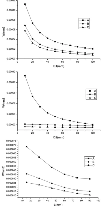
In order to acquire a better understanding of the variability in response due to the variation of inputs, 78 runs (26 runs for each diffuser sheets) were performed initially, prior to the start of optimization with D1 and D2 varying in a range from 10 to 100 mm, by 10 mm intervals and L varies between 15 and 90 mm, by 15 mm intervals.
The results illustrated in Fig. 4, have indicated that increasing D1, D2 and L, results in decreasing of the irradiance standard deviation. It also has been observed that the satisfying irradiance distribution is sensitive to variations of D1 and D2 both from 50 to 70 mm for L; it appeared to vary from 45 to 75 mm.
Therefore, the second simulation sets have been performed with 27 runs for each diffuser types, covering more sensitive parts to enhance the screening.
5. Optimization
Optimization has been done, using statistical analysis software to perform Design of experiments (4 Factors×3 Levels). DOE is a series of tests in which purposeful changes are made to the input variables of a system or
process and the effects on response variables are measured.
Design of experiments is applicable to both physical processes and computer simulation models. Experimental design is an effective tool for maximizing the amount of information gained from a study while minimizing the amount of data to be collected.9)
The results of DOE (Design of Experiments; Statistical Analysis) showed that contribution of inputs for type A in response variation is like, D2>D1>L, which means that L has the least and D1 has the most influences on uniformity.
Same results also have been achieved for type B and C. The contribution of each factor (source) in output variation rate is shown in Table 3. Undoubtedly, the optimized solution Table 2. factor setting for DOE
Factor Level
Diffuser type A B C
Distance between each adjacent
laser source (L) 50 mm 60 mm 70 mm
Distance between diffuser and bonded
wafer (D1) 50 mm 60 mm 70 mm
Distance between laser source and
diffuser (D2) 50 mm 60 mm 70 mm
1064 nm (collimated beam) laser source; Fixed Factor Output: Uniformity (irradiance distribution)
Fig. 4.The variation of Irradiance Distribution STDEV caused by variation of one variable while the other factors are fixed
for type C results in the best uniformity. The optimization results for type A, B and C are summarized in Table 4.
6. Speckle Contrast Reduction
When a coherent source illuminates an object that is rough on the scale of a wavelength, the interference of the many partial waves in the reflected light, with their random amplitudes and phases, produces the phenomenon known as
“speckle”.
In other words speckle is a random intensity pattern produced by the mutual interference of a set of wave-fronts.
This phenomenon has been investigated by scientists since the time of Newton to explain that twinkle stars, but speckles have come into prominence since the invention of the laser.
Researchers working in the fields of holography, holographic interferometry, laser microscopy, image processing, and synthetic aperture radar have seen the degradation of the image quality due to overlapped speckles. Since the speckling phenomenon exists inherently as long as the laser is used as an optical source in optical processing, the techniques of speckle reduction have been studied.
The methods of speckle reduction have been established in the past 30 years as one of the active research fields in coherent optical information processing. The history on studies of the speckle reduction started in the middle of 1960’'s with the quality improvement of images reconstructed from holograms by reducing the spatial coherence of illuminating light.
Theoretically the principles of speckle reduction may be classified as five categories: control of spatial coherence, control of temporal coherence, spatial sampling, spatial averaging, and digital image processing.
Speckle is usually quantified by the speckle contrast.
Speckle contrast reduction practically can be done by;
Angle diversity, Polarization diversity and Wavelength diversity. However there are some other alternatives such as rotating diffusers or moving/vibrating screens which can be used to reduce the speckle.
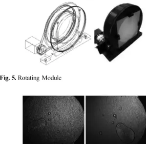
Rotating ground glass which destroys the spatial coherence of the laser light has several advantages compare to other solutions. It is easier and less expensive to manufacture also offers easier way to control the speckle contrast reduction ratio by altering the rotation speed. Fig. 5.
shows the CAD sketch and real configuration of manufactured rotating module for speckle contrast reduction in wafer bond inspection system.
Experiments have been done and effectiveness of rotating ground glass is confirmed. In Fig. 6 images before and after applying the rotating ground glass to the system are demonstrated and the speckle contrast obviously reduced and satisfying result is achieved by this method.
7. Result
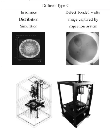
Defect Bonded wafer has been inspected by the system and clear image has been captured. Table 5 delivers a comparison between the raster chart of irradiance distribution created by optical design software through simulation, and the captured image.
8. Conclusion
Optimization has been done to develop the bonded wafer inspection system, and the feasibility of inspecting all area of the bonded surface simultaneously has been verified. Optical
Table 3. The contribution of each factor in output variation Contribution (%)
Source Type A Type B Type C
D2 72.12% 66.20% 57.38%
L 1.90% 0.71% 0.09%
D1 21.81% 8.90% 39.90%
Table 4. The final optimized cases for each diffuser type
D1 D2 L Irradiance STDEV
Type A 70 mm 70 mm 65 mm 2.15E-3 W/mm2 Type B 70 mm 70 mm 75 mm 1.13E-3 W/mm2 Type C 70 mm 70 mm 75 mm 0.94E-3 W/mm2
Fig. 5.Rotating Module
Fig. 6.Captured image before and after speckle contrast reduction
design software and statistical analysis software were used for simulation and optimization respectively. The CAD sketch and real image of the system is shown in Fig. 7.
Acknowledgment
This project is conducted through the Practical Application Project of Advanced Microsystems Packaging Program of Seoul Technopark, funded by the Ministry of Knowledge Economy.
References
1. S. T. Jung , K. S. Kim, S. P. Yang, H. C. Jung and Y. H. Lee,
“A Study on the Inner Defect Inspection for Semiconductor Package by ESPI”, Proc. KSME Fall conference, Muju Resort, 1442, The Korean Society of Mechanical Engineering (2003).
2. W. Chegal, Y. J. Cho, H. M. Cho, H. J. Kim, Y. W. Lee and S. H. Kim, “Measurement of Thin Film Thickness of Pat- terned Samples Using Spectral Imaging Ellipsometry”, Korean Society Of Precision Engineering, 21(6), 15 (2004).
3. S. J. Nam and K. S. Hahn, “Implementation of Automated Defect Detection and Classification System for Semiconduc-
tor Wafers”, The Korean Institute of Information Scientists and Engineers, 28(2), 334 (2001).
4. A. R. Burgers, R. Kinderman, J. D. Hylton, W. C. Sinke and H. H. C. De Moor, “Light-trapping in Saw-damage Etched Silicon Wafers”, ECN Solar Energy, 97(5), 30 (1997).
5. J. Zhao and M. A. Green, “Optimized Anti-reflection Coat- ings for High-Efficiency Silicon Cells”, IEEE T. Electron.
Dev., 38(8), 1925 (1991).
6. J. Hofstetter, C. del Canizo, S. Ponce-Alcantara and A. Luque
“Optimization of SiNx:H Anti-reflection Coatings for Silicon Solar Cells”, Spanish Conference on Electron Devices, 10(1109), 131 (2007).
7. W. D. Kelton, “Experimental Design for Simulation”, Winter Simulation Conference, 1(1), 32 (2000).
8. T. C. Urdan, Statistics in Plain English, 2nd Ed., pp.17, Lawrence Erlbaum Associates Publishers, Mahwah (2005).
9. J. K. Telford, “A Brief Introduction to Design of Experi- ments”, Johns Hopkins APL Technical Digest, 27(3), 224 (2007).
10. Z. Sun, J. Chang, N. Zhao, Weiqijin and Y.Wang, “Research of Diffusing Plates for LCD Backlights” Optik-International Journal for Light and Electron Optics, 121(8), 760 (2010).
11. J. W. Park, J. H. Lee, D. C. Shin and S. H. Park, “Luminance Uniformity of Large-Area OLEDs With an Auxiliary Metal Electrode”, Journal of Display Technology, 5(8), 306 (2009).
12. J. R. Ryu, B. H. Lee and G. Y. Lee, “Comparative Analysis of LED Array Methods to Improve a Luminous Intensity Uni- formity of LED Back Light in BLU” Korean Institute of Information Technology, 7(1), 4 (2009).
13. A. A. Ayon, X. Zhang, K. T. Turner, D. W. Choi, B. Miller, S. F. Nagle and S. M. Spearing, “Characterization of Silicon Wafer Bonding for Power MEMS Applications”, Sensors.
Actuat., 103(s 1-2), 1 (2003).
14. M. S. Kim and T. H. Baek, “Optical Measurement Using Laser Speckle Inferometry”, Journal of the Korean Society for Precision Engineering, 24(11), 38 (2007).
15. T. Iwai and O. Asakura, “Speckle Reduction in Coherent Information Processing”, Proceedings of the IEEE, 84(5), 766 (1996).
16. J. W. Goodman, “Speckle Phenomena in Optics: Theory and Applications”, pp.141-186, Roberts & Company Publishers, Greenwood Village (2007).
17. K. Hinkelmann, “Design and Analysis of Experiments: Intro- duction to Experimental Design”, 2, pp.45-70 John Wiley &
Sons Inc., Hoboken (2005).
18. Q. Wang, W. B. Kim, S. H. Choa, K. D. Jung, J. S. Hwang, M.
C. Lee, C. Y. Moon and I. S. Song, “Application of Au-Sn Eutec- tic Bonding in Hermetic RF MEMS Wafer Level Packaging”, J.
Microelectron. Packag. Soc., 12(3), 197 (2005).
19. J. H. Park, Y. M. Koo, E. K. Kim and G. S. Kim, “A Reli- ability and Warpage of Wafer Level Bonding for CIS Device Using Polymer”, J. Microelectron. Packag. Soc., 16(1), 27 (2009).
20. J. M. Kim, S. H. Kim and J. P. Jung, “Flip Chip Solder Joint Reliability of Sn-3.5Ag Solder Using Ultrasonic Bonding - Study of the Interface between Si-wafer and Sn-3.5Ag Sol- der”, J. Microelectron. Packag. Soc., 13(1), 23 (2006).
Table 5. Comparison Of Raster Chart Of Irradiance Distribution And Captured Image Of Bonded Wafer
Diffuser Type C
Irradiance Defect bonded wafer Distribution image captured by
Simulation inspection system
Fig. 7.Real image of the system