P1-54 / S.-H. Hong
• IMID 2009 DIGEST
Abstract
We present the epitaxial growth of high-quality ZnO layers by chemical vapor transport (CVT) technique on (01-12) sapphire with a ZnO buffer layer growth by metal-organic chemical vapor deposition (MOCVD). The surface of the grown ZnO epitaxial layers has atomically flats and the RMS is 0.11 nm. PL spectrum of as-grown samples exhibits two emissions originated by interactions between photon and free excitons.
1. Introduction
Zinc oxide (ZnO) is one of the most promising materials for fabricating in ultraviolet light emitting devices with high efficiency [1], and many researchers have concentrated their efforts on growing high quality ZnO epitaxial layers [2]. The absence of suitable substrates led many studies to perform hetero-epitaxial ZnO growth on a sapphire substrate. However, the quality of thin films is still worse. In the present study, we studied the ZnO epitaxial layer grown by the chemical vapor transport (CVT) method using carbon as a transport agent and high-purity ZnO source on the (01-12) sapphires substrate with a metal-organic chemical vapor deposition (MOCVD) grown ZnO buffer layer. The growth procedure was investigated, and the surface morphologies and optical properties of the grown epitaxial ZnO layers were evaluated.
2. Experimental
ZnO buffer layers were deposited on r-plane sapphire substrates (r-Al2O3) by metalorganic
chemical vapor deposition (MOCVD) with a
horizontal reactor. The substrate (r-plane sapphire) surface was degreased using ultrasonic cleaning in acetone, ethanol and rinsed with deionized water, and then etched by a chemical solution of H3PO4:
H2SO4=1:3 at 120
ºC
for 10min. After chemicalpolishing, the substrate was rinsed with deionized water, and dried. Zinc (DEZn) and pure oxygen (>99.99995%, O2) have been used as zinc and oxygen
sources, respectively.
The amount of DEZn transported to the reactor was set to 2×10⁻⁶ mol/min, and the flow rate of O
2 was set
to 8.9×10⁻⁴ mol/min. Total pressure of the reactor was
kept at 70Torr and the ZnO buffer layer was grown at 400
ºC
. After growth, to improve surface smoothness and crystalline quality, thermal treatment of ZnO buffer layer was carried out by annealing under a flow of 0.1 MPa O2 at 900ºC
for 1h.The main ZnO layer was deposited under the growth temperature of 960
ºC
for 12h by CVT method using carbon as a transport agent and high-purity ZnO source. We designed a configuration of the CVT ampoules as well as our previous report [3].Surface morphology of the buffer layer and epitaxial layers were characterized using atomic force microscopy (AFM) (SPA400 system by Seiko Instruments Inc.). The optical property of ZnO epitaxial films were evaluated by low temperature photoluminescence (PL). The measurement of the photoluminescence (PL) spectra was performed at 8 K by using He-Cd laser (325nm) as the excitation light source.
3. Results and discussion
Figure 1 shows the AFM images of the annealed MOCVD-ZnO buffer layer surfaces. The surface of annealed MOCVD-ZnO buffer layer exhibits regular
Fabrication of epitaxial ZnO layers on MOCVD-ZnO/(01-12)
sapphire by chemical vapor transport
Sang-Hwui Hong
1, Kenichi Kato
1, Kouji Mimura
1, Masahito Uchikoshi
1,
Seishi Abe
2and Minoru Isshiki
11Institute of Multidisciplinary Research for Advanced Materials, Tohoku University,
Katahira 2-1-1, Aoba-ku, Sendai 980-8577, Japan
Tel.:81-22-217-5139, E-mail: [email protected]
2The Research Institute for Electric and Magnetic Materials, 2-1-1 Yagiyama-minami,
Sendai 982-0807, Japan
P1-54 / S.-H. Hong
IMID 2009 DIGEST • steps aligning with a root mean square roughness of
1.1 nm. The MOCVD-ZnO/(01-12) sapphire was used as a substrate of ZnO epitaxial layer growth.
Fig. 1. AFM images of MOCVD-ZnO surface pretreated at 900
ºC
for 1h in O2 atmosphere.The AFM image of epitaxial ZnO layer grown on MOCVD-ZnO/(01-12) sapphire is shown in Fig. 2. Deposition time was 24 h. The smooth surface with a root means surface (RMS) roughness of 0.11nm was obtained. The line scan reveals a step height of 0.2 nm. These results indicate that the surface morphology of epitaxial layer was significantly improved after epitaxial growth by CVT method.
Fig. 2. The related AFM image of the scan area 5 × 5 µm2 is displaying epitaxial layers steps.
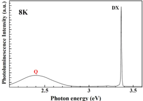
Photoluminescence measurement was carried out for inquiring the quality of ZnO epitaxial layer. Fig. 3 show a PL spectrum of the ZnO epitaxial layer in the range of 2.1 to 3.6 eV. The PL spectrum indicates a sharp excitonic emission (DX) at about 3.37 eV. The Q peak is observed around 2.40 eV as shown in Fig. 3.
This is so-called green emission. The similar peak position is also reported by M. Mikami et al. [4], which has been controversial for argument among researchers for decades.
Fig. 3. Photoluminescence spectrum of epitaxial ZnO layer in the range of 2.1 to 3.6 eV at 8 K.
Fig. 4. Photoluminescence spectrum of epitaxial ZnO layer at 8 K.
Figure 4 shows the PL spectrum measured in the range of 3.325 to 3.425 eV at 8 K. The PL spectrum shows several bound-exciton peaks. Teke et al. [5] reported that these emissions are related to excitons bound to neutral or ionized donors. The prominent lines are positioned at 3.3632 (I4), 3.3651 (I3), and
3.3701 (I1) eV. However, donor-type impurities such
as Al, Ga, and In identified by the studies of Meyer et
al. [6] were not observed in Fig. 4. However, two
peaks were observed at 3.3775 and 3.3832 eV, and these peaks were identified in the studies of Reynolds
et al. [7] and Chichibu et al. [8] as emissions from the
A-free exciton and its first excited state emission at 3.3775 eV and lower B excitonic polariton branches (LPBB) at 3.3832 eV.
P1-54 / S.-H. Hong
• IMID 2009 DIGEST
These results demonstrate that the epitaxial ZnO layers are of high purity and good crystallinity.
4. Summary
We have succeeded to grow high-quality ZnO epitaxial layers by chemical vapor transport (CVT) technique on (01-12) sapphire with a ZnO buffer layer growth by metal-organic chemical vapor deposition (MOCVD). The surface of the grown ZnO epitaxial layers has atomically flats and the RMS is 0.11 nm. Photoluminescence measurements demonstrate that the grown ZnO epitaxial layer is of high purity and good crystallinity.
Acknowledgement
This work was supported by Global COE Program “Materials Integration (International Center of Education and Research), Tohoku University,” under MEXT, Japan.
5. References
1. D. Bagnal, Y.Chen, Z. Zhu, T. Yao, S. Koyama, M. Shen and T. Goto, Appl. Phys. Lett. 70, p.2230 (1997).
2. K.-I. Ogata, K. Maejima, Sz. Fujita and Sg. Fujita,
J. Cryst. Growth 248, p.25 (2003).
3. S.-H. Hong, M. Mikami, K. Mimura, M. Uchikoshi, A. Yasuo, S. Abe, K. Masumoto and M. Isshiki, J. Crystal Growth 311, p.3609 (2009). 4. M. Mikami, S.-H. Hong, T. Sato, S. Abe, J. Wang,
K. Masumoto, Y. Masa and M. Isshiki, J. Crystal
Growth 304, p.37 (2007).
5. A. Teke, Ü. Özgür, S. Doğan, X. Gu and H. Morkoç, B. Nemeth, J. Nause and H. O. Everitt,
Phys. Rev. B 70, p.195207 (2004).
6. B. K. Meyer, H. Alves, D. M. Hofmann, W. Kriegseis, D. Forster, F. Bertram, J. Christen, A. Hoffmann, M. StraBburg, M. Dworzak, U. Haboeck and A. V. Rodina, Phys. Stat. Sol. (b) 241, p.231 (2004).
7. D. C. Reynolds, D.C. Look, B. Jogai and T. C. Collins, Appl. Phys. Lett. 79, p.3794 (2001). 8. S. F. Chichibu, T. Sota, G. Cantwell, D. B. Eason