44-4 / S. –W. Lee
IMID 2009 DIGEST •
a-Si Process-based Advanced SPC TFT for AMOLED Application
Seok-Woo Lee*, Sang-Jin Lee, Tae-Joon Ahn, Soo-Jeong Park,
Suhyuk Kang, Sang-Hoon Jung, Hong-Koo Lee, Sung Ki Kim, Yong In Park,
Chang-Dong Kim, Myoung-Su Yang, In Byeong Kang, and Yong-Kee Hwang
LG Display R&D Center, 1007, Deogeun-ri, Wollong-myeon,
Paju-city, Gyeonggi-do, 413-811, Korea
Phone: +82-31-933-5440 , E-mail: [email protected]
Keywords : a-SPC, top gate, AMOLED, Backplane
Abstract
a-Si process-based advanced-SPC (a-SPC) TFT has been developed and verified by manufacturing an AMOLED panel having improved cost competitiveness by using the existing a-Si infrastructure. The a-SPC TFT had superior device reliability and current drivability to a-Si TFT to meet the requirements of AMOLED backplane.
1. Introduction
Active matrix organic light emitting diode (AMOLED) displays have attracted considerable attention among flat panel displays due to high brightness characteristics with low power consumption, light weight, fast response time and wide viewing angle.1) Recently, amorphous silicon thin film transistor (a-Si TFT) based AMOLED displays have been reported, with good uniformity in large size panel.2) However, improving poor stability of a-Si TFTs have been well known to be a much more difficult problem than achieving the uniformity of polycrystalline silicon (poly-Si) TFT based on the laser crystallization.
The poly-Si TFTs have higher mobility and better stability than the a-Si TFTs, however, the production cost is relatively high and there is also short range non-uniformity issue. On the other hand, the a-Si TFTs have good uniformity and low cost process, but they have poor stability over time under the electrical stress. In order to achieve high yield and cost effectiveness for mass production of AMOLED displays, the backplane having simple, stable, and uniform device characteristics should be developed.3)
In this work, a top-gate structure TFT employing the advanced solid phase crystallization (a-SPC) is introduced based on the conventional a-Si TFT processes, which meets most of the requirements for the backplane of AMOLED displays.
2. Experimental
Top gate n-type TFTs were fabricated on Corning E2k glass substrate without any issue in process. Figure 1 shows process sequence of the top gate n-type TFT with a-SPC process named hereafter as T/G a-SPC TFT.
Firstly, a 50 nm-thick amorphous silicon was deposited on the SiO2/SiN buffer layer by plasma enhanced chemical vapor deposition (PECVD) as a precursor. Then, a-SPC process was applied at maximum 750 ℃ to crystallize the precursor layer.3) The alternating magnetic field adopted in the a-SPC process is known to induce eddy current that generates joule heat on the precursor amorphous silicon film. The induced joule heat increased the temperature especially on the amorphous precursor layer during crystallization, which leads to superior crystallinity to conventional SPC samples. After the crystallization, a 30 nm-thick optimized n+ a-Si layer was successfully deposited and patterned.
44-4 / S. –W. Lee
• IMID 2009 DIGEST
Buffer & Active depo.
A-SPC
N+depo.
Active patterning
Gate Insulator depo.
Gate depo. & patterning
Passi depo. & patterning
ITO depo. & patterning
Bank patterning
OLED process S/D depo. & patterning
N+etch
Figure 1. Major process sequence of the proposed T/G a-SPC TFT.
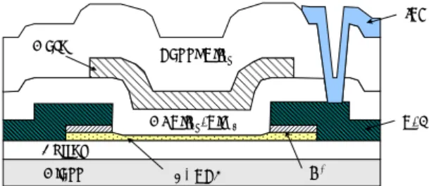
Secondly, a source/drain metal layer was deposited and patterned onto the pre-patterned active layer. The n+ layer was dry etched with PR mask to define TFT channel region. Thirdly, a stacked gate insulator layer (SiO2/SiNx = 2000/500Å) and a 200 nm-thick gate metal were sequentially deposited and patterned. Fourthly, 30 nm-thick SiNx was deposited as a passivation layer and contact hole pattern was performed by conventional dry etch process. Finally, ITO layer was formed. The cross-sectional view of the fabricated TFT structure is shown in Figure 2.
ITO GI S iNx/S iO2 Pas si S iNx G at e S/ D A- S PC Gla ss B uffer N+
Figure 2. Device structure of T/G a-SPC TFT.
3. Results and Discussion
The electrical transfer characteristics of TFTs were measured at room temperature with the drain-source voltage Vds=0.1 V and Vds=10.0 V, with the variation of the gate voltage Vg from -15.0 to +20.0 V. Figure 3 shows comparison of transfer curves between a-Si TFT and T/G a-SPC TFT. As shown in the transfer curves, the T/G a-SPC TFT showed higher current drivability than that of the a-Si TFT. The T/G a-SPC TFTs have maximum field effect mobility of 9 cm2/Vs, which is around 23 times higher than that of a-Si TFTs. -15 -10 - 5 0 5 10 15 20 1E -14 1E -13 1E -12 1E -11 1E -10 1E -9 1E -8 1E -7 1E -6 1E -5 1E -4 1E -3 Vd s=10.0V a-Si TFT
top g ate A-SPC TFT
I ds (A ) Vgs (V) Vds=0.1V W/L=6/6um (uFE~9.0cm 2/Vs) W/L=36/6um (uFE~0.4cm 2/Vs)
Figure 3. Comparison of transfer curves between a-Si TFT and T/G a-SPC TFT.
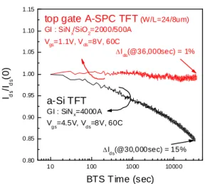
In order to examine the reliability characteristics, bias-temperature stress (BTS) were measured at saturation condition. Figure 4 shows the comparison of drain current degradation between a-Si TFT and T/G a-SPC TFT under the BTS stress as a function of the stress time. As shown in the figure, the current degradation after applying the BTS was about 1% for T/G a-SPC TFT, which was much smaller than 15% of a-Si TFT.
44-4 / S. –W. Lee IMID 2009 DIGEST • 10 100 1000 10000 0.80 0.85 0.90 0.95 1.00 1.05 1.10 1.15 a-Si TFT GI : SiNx=4000A Vgs=4.5V, Vds=8V, 60C I ds /I ds (0 ) BTS T ime (sec)
top gate A-SPC TFT (W/L=24/8um) GI : SiNx/SiO2=2000/500A
Vgs=1.1V, Vds=8V, 60C
∆Ids(@30,000sec) = 15%
∆Ids(@36,000sec) = 1%
Figure 4. Comparison of Ids variation under bias temperature stress between a-Si TFT and T/G a-SPC TFT.
The availability of T/G a-SPC TFTs for AMOLED backplane was also verified by manufacturing a 15” XGA bottom emission AMOLED panel as shown in Figure 5, and Table 1 shows the specification of the panel. Using the relatively higher current drivability of a-SPC TFT, a bottom emission panel adopting 5T-1C compensation circuit was successfully developed with 40% of aperture ratio.
Figure 5. Image of a 15” Bottom Emission AMOLED panel with T/G a-SPC TFT backplane.
Table 1. Specification of 15” AMOLED panel.
40% Aperture ratio 5T-1C Pixel structure Bottom emission Display type RGB vertical stripe Pixel arrangement 1024×RGB×768 Resolution 99um×297um×3 (85.5ppi) Pixel pitch 15 inch Diagonal size 304.13mm(H)×228.10mm(V) Panel dimension Spec. Feature 40% Aperture ratio 5T-1C Pixel structure Bottom emission Display type RGB vertical stripe Pixel arrangement 1024×RGB×768 Resolution 99um×297um×3 (85.5ppi) Pixel pitch 15 inch Diagonal size 304.13mm(H)×228.10mm(V) Panel dimension Spec. Feature
4. Summary
We have developed the top-gate structure n-type TFT employing a-SPC based on the conventional a-Si TFT processes and a 15-inch AMOLED panel was manufactured for the verification of the T/G a-SPC TFT. It showed that the T/G a-SPC TFTs could be one of the strong candidates for a backplane of AMOLED displays due to their superior reliability and current drivability compared to the a-Si TFTs and lower cost process compared to the poly-Si TFTs.
5. References
[1] C. W. Tang, SID Int. Symp. Dig. Tech. Pap., 181 (1996).
[2] T. Tsujimura, Y. Kobayashi, K. Murayama, A. Tanaka, M. Morooka, E. Fukumoto, H. Fujimoto, J. Sekine, K. Kanoh, K. Takeda, K. Miwa, M. Asano, N. Ikeda, S. Kohara, and S. Ono, SID Int. Symp. Dig. Tech. Pap., 6 (2003).
[3] S.H. Kang, T.J. Ahn, S.J. Park, S.W. Lee, C.Y. Kim, C.D. Kim. I.B. Kang, AM-FPD 07, 203 (2007).
[4] M.-Y. Chang, C.-T. Peng, J.-Y. Lin, C.-H. Lin, AM-FPD 06, 301 (2006).