P2-82 / D. Y. Kim
• IMID 2009 DIGES
Abstract
In this paper, the etching behavior of ZnO in CF4 plasma mixed Ar was investigated. Previously, the etch rate in CF4/Ar plasma was reported that it is slower than that in Cl containing plasma. But, plasma included Cl atom can produce the by-product such as ZnCl2. In order to solve this film contamination, no Cl containing etching gas is required. We controlled the etching parameter such as source power, substrate bias power, and CF4/Ar gas ratio to acquire the fast etch rate using a ICP etcher. We accomplished the etching rate of 144.85 nm/min with the substrate bias power of 200W. As the energetic fluorine atoms were bonded with Zinc atoms, the fluoride zinc crystal (ZnF2) was observed by X-ray photoelectron spectroscopy (XPS).
1. Introduction
ZnO is an II–VI semiconductor oxide with a direct band gap of 3.3 eV. Besides the wide band gap, ZnO has several interesting properties, such as large exciton binding energy, high chemical stability, good piezoelectric properties [1], non-toxicity and bio-compatibility [2], which have greatly considered since a few decade years ago [3]. Among the optical advantages, ZnO has the larger exciton binding energy of 60 meV than that of gallium nitride (28 meV) and of zinc selenide (19 meV). This makes it possible to observe exciton radiative recombination at room temperature [4]. ZnO thin films also can be applied in fabrication of hydrogenated amorphous silicon solar cells [5] because of self-textured surface without additional process and a stability in hydrogen plasma. Additionally, ZnO thin films have potential for practical applications, active layer of field effect transistor, especially in high mobility thin film transistor for silicon on panel [6]. ZnO also has very simple crystal growth technology in comparison to other semiconductor devices, resulting in an available lower cost for ZnO based devices. Most important applications include the transparent electrode for
photovoltaic device like a solar cells [7] and active layer of switching device for flat panel displays [8], and a gas sensors [9]. For the microelectronic and photovoltaic device application, ZnO dry etching techniques with high etch rates, high selectivity over mask materials, and highly anisotropic etch profiles is very important. Lee et al. reported inductively coupled plasma (ICP) dry etching behaviors in CH4-based
plasma that a high etch rate of ZnO could be obtained by increasing ICP and r.f. powers [10]. Kim et al. also exhibited the etch mechanism for ZnO in ICP plasma
chemistries of BCl3-based plasma [11]. The
optimization of dry etching processes for ZnO is very important to fabricate microelectronic device included ZnO device. However, there are very few reports describing the dry etching of ZnO using a CF4 mixed
by Ar plasma sources because of their slow etch rate. Generally, Cl2 or BCl3 is used as etch gas to reach the
fast etch rate. However, these leave a great problem of Cl contamination such as ZnCl2. It can be possible to
make a trouble in the device operation. In this paper, we suggested the CF4-based plasma etching using a
ICP system.
2. Experimental
Undoped ZnO films were grown on (100) silicon substrates by low temperature chemical vapor deposition (LPCVD) systems at the 200 °C using a diethyl-zinc (DEZ) and oxygen gas. The prepared ZnO samples were etched in a load locked ICP system (manufactured by SNTEK Co. Korea). We illustrated the schematic diagram and electric field of ICP etching system in the Fig. 1. The plasma is generated by circular coil antenna and forced toward substrate by substrate bias voltage. The plasma density can be generated by a 13.65 MHz rf power supply controlling the ICP coil power, while the ion energy can be controlled by a 13.56 MHz rf power supplier applied to the substrate. As shown the Fig. 1(b), plasma
Dry etching of ZnO thin film using a CF
4mixed by Ar
Do Young Kim*, Hyungjun Kim
Dept. of Materials Science and Engineering, POSTECH, Pohang, 790-784, Korea Tel.:82-54-279-5465, E-mail: [email protected]
P2-82 / D. Y. Kim
IMID 2009 DIGES •
electric field forms the disc-like shape under ICP coil. Etch rates were investigated as a function of CF4/Ar
chemistry and substrate bias power. Film thickness was measured by spectroscopy ellipsometry (Elli-SE, Ellipso tech. Co.). X-ray photon spectroscopy (XPS, VG instrument Korea, ESCALAB 2201) was performed to investigate the surface chemical contents of ZnO before and after etching.
Fig. 1 The schematic of ICP etching system (a) plasma generation system and (b) electric field distribution and ion acceleration direction.
3. Results and discussion
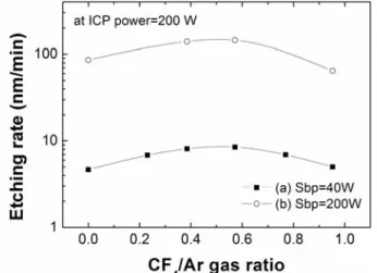
Fig. 2(a) shows the etch rate of ZnO as a function of the CF4/Ar gas mixture under the surface bias
power (Sbp) of 40 W. It is noted that etch rate is slightly increased from 4.65 to 8.53 nm/min as the CF4/Ar gas ratio increases. However, etch rate
decreased from 8.53 to 5.01 nm/min as the CF4/Ar gas
ratio increases above 0.57. Fig. 2(b) shows the etch rate of ZnO as a function of CF4/Ar gas ratio at the
Sbp of 200 W at the room temperature. As the Sbp increases from 40 W to 200 W, etch rate sharply increased by 17 times. As the CF4/Ar gas ratio is
increased, the etch rate is not only slightly increased from 86 to 144.85 nm/min but also decreased from 144.85 to 64.62 nm/min to more than CF4/Ar gas ratio
of 0.57. This result shows the same tendency with that of Fig. 2(a). It indicates that the etch rate of ZnO is considerably dependent on the Sbp. However, CF4/Ar
gas ratio has a little related with etch rate [12]. The highest etch rate is obtained when proceed with the Sbp of 200 W and CF4/Ar gas ratio of 0.57. This result
shows that the CF4 plasma is effective in etching ZnO,
compared to Ar or Cl2/Ar plasmas[11].
Fig. 3 shows the etch rates of ZnO as a function of Sbp in the CF4/Ar gas ratio which is 0.38 and 0.57,
respectively. The ICP coil power was maintained at
200 W. As the Sbp is increased, the ZnO etch rate was increased like a square function, reaches a maximum at 200 W. This etching behavior exhibits that the Sbp plays an important role in etching ZnO by the acceleration of ion such as F atoms and CFx radicals
[12]. However, Woo et al. reported that the etch rate of ZnO with small addition of CF4 gas ratio can be
attributed to at least two effects connected to both volume and surface chemistries. The first is effective removal of O from the surface of ZnO resulting ion sputtering yield. The second is the reson that slow etch rate of ZnO is related with a decrease in the efficiency of ion-stimulated desorption of reaction products because of high melting points for etch by products (ZnF2=872 °C) [13]. However, our result was
different with it of Woo et al. We achieved the fast etch rate around 145 nm/min, which should mean that the chemical etching behavior is different from previous report.
Fig. 2 ZnO etching rate as a function of CF4/Ar gas
ratio (a) Sbp=40 W, (b) Sbp=200 W.
Fig. 3 ZnO etching rate as a function of Sbp (a)
P2-82 / D. Y. Kim
• IMID 2009 DIGES
For further detailed investigations of chemical reaction between ZnO and F atoms or CFx radicals
before and after plasma etching, XPS analysis was performed. Fig. 4(a) and (b) show XPS narrow scan analysis for Zn 2p and O 1s before and after etching in CF4/Ar plasma. In order to investigate the chemical
states, the etched ZnO surfaces were compared with as-grown one. As shown in Fig. 4(a), for the as-grown ZnO film, the Zn 2p peak can separate into two peaks at binding energies of 1044.8 eV (Zn 2p1/2) and 1021.8 eV (Zn 2p3/2), respectively[14]. After etching in CF4/Ar plasma, the Zn 2p peaks shifted by 1 eV
toward higher binding energy. As reported in [14], this binding energy shift was caused by the changes of the surface Fermi level of ZnO toward conduction band edge and the accumulation of Zn-F bonds. The O 1s peak also consisted of two maximums at 530.7 eV and 532.2 eV before ZnO etching. For O 1s peak after the introduction of CF4/Ar plasma, the intensity at 530.1
eV drastically decreased with increasing the CF4/Ar
gas ratio. After etching in CF4/Ar plasma, the intensity
at 532.2 eV was not only increased with increasing the CF4/Ar gas ratio, but also moved by 0.6 eV toward
higher binding energy. From these observations, we can consider that the Zn-O bonds are effectively broken by the CFx radicals from decreasing the peak
of 530.7 eV with increasing of CF4/Ar gas ratio. The F
1s peak exhibits only one maximum value of 685.8 eV. This peak is related the fluoride crystal, ZnF2 [15].
From the ref. [15], the peak of ZnF2 was 685.1±0.1 eV.
However, our binding energy of ZnF2 had a difference
of about 0.7 eV. This reason might be due carbon bonding with ZnO as shown in the Fig 4(d). For the as-grown one, F 1s peak was not observed. This peak indicates that energetic F atoms generated by CFx
radical made Zn-F bonds with zinc atom since Sbp induced to force ion acceleration toward substrate.
Fig. 4 (a) Zinc 2p, (b) oxygen 1s, (c) fluorine 1s, and (d) carbon 1s binding energy measured by XPS narrow scan.
Fig. 4(d) shows that the intensities of the C 1s spectra from the different CF4/Ar gas ratio and sample
before the etching. The peaks related in carbon contamination (C=C) and hydrogenated carbon (C-H) were observed in the around 289 eV and 295 eV
P2-82 / D. Y. Kim
IMID 2009 DIGES •
respectively [16]. From our observation, carbon contamination has no large difference as a function of
CF4/Ar or sample before the etching. However,
hydrogen carbon bonding was decreased with starting the CF4 plasma etching. This result implies the
removal of carbon atoms from the surface by the formation of the by-products like a Zn compound, Zn(CFx)y. Finally, Zn compound is removed by Ar+
ion bombardment forced the Sbp.
4. Summary
In this study, we carried out experimental investigations of ZnO etching behavior in CF4/Ar,
plasma. We have figured that an increase of the CF4/Ar gas ratio slightly leads to an increase in etch
rate. However, Sbp is mainly predominant the etch rate, which reaches a maximum value of 144.85 nm/min at the Sbp of 200 W. From the results of XPS analysis, the non-volatile by product such as Zn-F bonds was observed in CF4/Ar plasma. However, the
Zn-F bonds play no important role of etching rate. To conclude, ZnO film produces the formation of the Zn organic compound which is removed by energetic Ar+ bombardment.
Acknowledgement
This work was supported by Korea Research Foundation (KRF-2007-331-D00243, and KRF-2008-005-J00501) and the Korea Science and Engineering Foundation (KOSEF, R01-2007-20143-3 and No. 2007-02864).
5. References
1. J. Zhou, Y. Gu, P. Fei, W. Mai, Y. Gao, R. Yang, G. Bao, and Z.L. Wang, Nano Lett., 8[9], p.3035 (2008).
2. Y.L. Wu, C.S. Lim, S. Fu, A.I.Y. Tok, H.M. Lau, F.Y.C. Boey, and X.T. Zeng, Nanotechnol., 18[21], p.215604 (2007).
3. U. Ozgur, Y.I. Alivov, C. Liu, A. Teke, M.A. Reshchikov, S. Dogan, V. Avrutin, S.J. Cho, and H. Morkoc, J. Appl. Phys., 98[4], p.041301 (2005). 4. Makoto Kurimoto, A. B. M. Almamun Ashrafi,
Masato Ebihara, Katsuhiro Uesugi, Hidekazu Kumano, and Ikuo Suemune, Phys. Status Solidi B,
241[3], p.635 (2004).
5. W. Beyer, J. Hukes, and H. Stiebig, Thin Solid
Films, 516[2-4], p.147 (2007).
6. E.M.C. Fortunato, P.M.C. Barquinha, A.C.M.B.G. Pimentel, A.M.F. Goncalves, A.J.S. Marques, R.F.P. Martins, and L.M.N. Pereira, Appl. Phys.
Lett., 85[13], p.2541 (2004).
7. S. Fay, L. Feitknecht, R. Schluhter, U. Kroll, E. Vallat-Sauvain, and A. Shah, Sol. Energy Mater.
Sol. Cells, 90[18-19], p.2960 (2006).
8. B.Y. Oh, M.C. Jeong, T.H. Moon, W. Lee, J.M. Myoung, J.Y. Hwang, and D.S. Seo, J. Appl. Phys.,
99, p.124505 (2006).
9. T. Miyata, T. Hikosaka, and T. Minami, Sensors &
Actuators: B. Chemical, 69[1-2], p.16 (2000).
10. J.M. Lee, K.M. Chang, K.K. Kim, W.K. Choi, and S.J. Park, J. Electrochem. Soc., 148[1], p.G1 (2001).
11. H.K. Kim, J.W. Bae, K.K. Kim, S.J. Park, T.Y. Seong, and I. Adesida, Thin Solid Films, 447-448, p.90 (2004).
12. A.M. Efremov, D.P. Kim, and C.I. Kim, Vacuum,
75[2], p.133 (2004).
13. J.C. Woo, G.H. Kim, J.G. Kim, and C.I. Kim, Surf.
Coat. Technol., 202, p.5705 (2008).
14. S.W. Na, M.H. Shin, Y.M. Chung, J.G. Han, and N.E. Lee, J. Vac. Sci. Technol. A, 23[4], p.898 (2005).
15. Y. Kawamoto, K. Ogura, M. Shojiya, M.
Takahashi, and K. Kadono, J. Fluorine Chem.,
96[2], p.135 (1999).
16. M.H. Shin, M.S. Park, S.H. Jung, J.H. Boo, and N.E. Lee, Thin Solid Films, 515[12], p.4950 (2007).