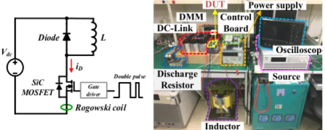
L iD Vdc Rogowski coil Gate driver Double pulse Diode SiC MOSFET DMM Control Board DC-Link Discharge Resistor DUT Oscilloscope Inductor Source Power supply
그림1 Double pulse test회로도 및 실험 환경 Fig. 1 Circuit diagram of double pulse test and
experimental environment.
196
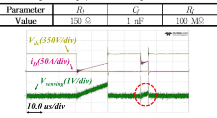
표 1 Double pulse test bed사양 Table 1 Specifications of double pulse test
iD M + –MdiD/dt La c c – + Ra Ca R1 Rf Cf + –Vsensing 그림2 Rogowski코일 회로도
Fig. 2 Rogowski coil circuit diagram.
× ×
×
≥ × ×
× min 표 2 Rogowski코일 회로의 적분기 설계 파라미터Table 2 Integrator design parameters of Rogowski coil circuit
Ω Ω iD M + –MdiD/dt La c c – + Ra Ca R1 Rf Cf + –Vsensing Rin c Cin Input filter 그림4입력 필터를 적용한Rogowski코일 회로도 Fig. 4 Rogowski coil circuit diagram with input filter.
-50 0 50 100 150 -1.1 0 1.1 2.2 3.3 200 [MHz] 66 [MHz] 30 [MHz] 14 [MHz] 9.7 [MHz] Drain current
V
se ns in g[V
]
i
D[
A
]
Time
그림5입력 필터의 대역폭 변화에 따른 적분기 출력(Vsensing)파형 Fig. 5 Waveforms of integrator output(Vsensing) depending onbandwidth variation of input filter. Vdc(350V/div)
iD(50A/div)
Vsensing(1V/div) 10.0 us/div
그림3 Double pulse test파형 Fig. 3 Waveforms of double pulse test.
-iD M + –MdiD/dt La c c – + Ra Ca R1 Rf Cf + –Vsensing Rin c Cin Rout c Cout Output filter 그림6출력 필터를 적용한Rogowski코일 회로도
Fig. 6 Rogowski coil circuit diagram with output filter.
-50 0 50 100 150 -1.1 0 1.1 2.2 3.3 70 [MHz] 23 [MHz] 10 [MHz] 5 [MHz] 3.4 [MHz] Drain current
V
se n si n g[V
]
i
D[
A
]
Time
그림7출력 필터의 대역폭 변화에 따른 적분기 출력(Vsensing)파형 Fig. 7 Waveforms of integrator output(Vsensing) depending onbandwidth variation of output filter.
그림8턴 수에 따른Rogowski코일 회로
Fig. 8 Rogowski coil circuit according to the number of turns.
-0.5 0 0.5 1 1.5 2 2.5 125 turns 90 turns 72 turns
V
se ns in g[V
]
i
D[
A
]
그림9 Rogowski 코일 턴 수에 따른 적분기 출력 파형Fig. 9 Integrator output(Vsensing) waveforms with Rogowski coil turns.
Drain current
Rogowski
coil
그림10 턴 수에 따른 상호 인덕턴스 도출을 위한 모델 및 시뮬레이션 결과Fig. 10 Simulation model and results for deriving mutual inductance according to the number of turns.