Multilayer transparent electrode for organic
light-emitting diodes: tuning its optical
characteristics
Hyunsu Cho, Changhun Yun, and Seunghyup Yoo*
Department of Electrical Engineering, Korea Advanced Institute of Science and Technology (KAIST), 373-1 Guseong-dong, Daejeon 305-701, Republic of Korea
Abstract: The optical properties of dielectric-metal-dielectric (DMD) transparent electrodes are investigated from the perspectives of organic light-emitting diodes (OLEDs). A joint experimental and theoretical study showed that the optical characteristics of OLEDs based on DMD electrodes can be widely tuned to fulfill the requirements of a target application through careful control of the microcavity effect, transmittance of DMD electrodes, and a correlation of these two factors with the emission spectra of the emitted materials. Upon variation of the DMD structure, near-Lambertian emission and a 100% improvement in the luminous efficiency are demonstrated, respectively. Optimization strategies are also discussed that are relevant to forward luminous efficiency, total optical power, and angular/ spectral characteristics.
©2010 Optical Society of America
OCIS codes: (230.3670) Optical devices: Light-emitting diodes; (230.4170) Optical devices: Multilayer; (310.4165) Thin films: Multilayer design; (310.6860) Thin films; Thin films, optical properties.
References and links
1. P. E. Burrows, G. Gu, V. Bulovic, Z. Shen, S. R. Forrest, and M. E. Thompson, “Achieving Full-Color Organic Light-Emitting Devices for Lightweight, Flat-Panel Displays,” IEEE Trans. Electron. Dev. 44(8), 1188–1203 (1997).
2. B. W. D’Andrade, and S. R. Forrest, “White Organic Light-Emitting Devices for Solid-State Lighting,” Adv. Mater. 16(18), 1585–1595 (2004).
3. G. F. Wang, X. M. Tao, and R. X. Wang, “Flexible organic light-emitting diodes with a polymeric nanocomposite anode,” Nanotech. 19(14), 145201 (2008).
4. H. Pang, Y. Yuan, Y. Zhou, J. Lian, L. Cao, J. Zhang, and X. Zhou, “ZnS/ Ag/ ZnS coating as transparent anode for organic light emitting diodes,” J. Lumin. 122–123, 587–589 (2007).
5. H. Cho, C. Yun, J.-W. Park, and S. Yoo, “Highly flexible organic light-emitting diodes based on ZnS/Ag/WO3 multilayer transparent electrodes,” Org. Electron. 10(6), 1163–1169 (2009).
6. C. Yun, H. Cho, H. Kang, Y. Lee, Y. Park, and S. Yoo, “Electron injection via pentacene thin films for efficient inverted organic light-emitting diodes,” Appl. Phys. Lett. 95(5), 053301 (2009).
7. J. Lewis, S. Grego, B. Chalamala, E. Vick, and D. Temple, “Highly flexible transparent electrodes for organic light-emitting diode-based displays,” Appl. Phys. Lett. 85(16), 3450 (2004).
8. X. Liu, X. Cai, J. Qiao, J. Mao, and N. Jiang, “The design of ZnS/ Ag/ ZnS transparent conductive multilayer films,” Thin Solid Films 441(1-2), 200–206 (2003).
9. J. C. C. Fan, and F. J. Bachner, “Transparent heat mirrors for solar-energy applications,” Appl. Opt. 15(4), 1012– 1017 (1976).
10. S. Y. Ryu, J. H. Noh, B. H. Hwang, C. S. Kim, S. J. Jo, J. T. Kim, H. S. Hwang, H. K. Baik, H. S. Jeong, C. H. Lee, S. Y. Song, S. H. Choi, and S. Y. Park, “Transparent organic light-emitting diodes consisting of a metal oxide multilayer cathode,” Appl. Phys. Lett. 92(2), 023306 (2008).
11. H. A. Macleod, Thin-film optical Filters (Taylor & Francis, 2001).
12. D. G. Deppe, C. Lei, C. C. Lin, and D. L. Huffaker, “Spontaneous emission from planar microstructures,” J. Mod. Opt. 41(2), 325–344 (1994).
13. M. Thomschke, R. Nitsche, M. Furno, and K. Leo, “Optimized efficiency and angular emission characteristics of white top-emitting organic electroluminescent diodes,” Appl. Phys. Lett. 94(8), 083303 (2009).
14. S. Han, W. Shin, M. Seo, D. Gupta, S. Moon, and S. Yoo, “Improving performance of organic solar cells using amorphous tungsten oxides as an interfacial buffer layer on transparent anodes,” Org. Electron. 10(5), 791–797 (2009).
15. J. Meyer, S. Hamwi, T. Bulow, H.-H. Johannes, T. Riedl, and W. Kowalsky, “Highly efficient simplified organic light emitting diodes,” Appl. Phys. Lett. 91(11), 113506 (2007).
16. C. Tao, S. Ruan, G. Xie, X. Kong, L. Shen, F. Meng, C. Liu, X. Zhang, W. Dong, and W. Chen, “Role of tungsten oxide in inverted polymer solar cells,” Appl. Phys. Lett. 94(4), 043311 (2009).
17. H. Riel, S. Karg, T. Beierlein, W. Rieß, and K. Neyts, “Tuning the emission characteristics of top-emitting organic light-emitting devices by means of a dielectric capping layer: An experimental and theoretical study,” J. Appl. Phys. 94(8), 5290 (2003).
18. J. Lim, S. S. Oh, D. Y. Kim, S. H. Cho, I. T. Kim, S. H. Han, H. Takezoe, E. H. Choi, G. S. Cho, Y. H. Seo, S. O. Kang, and B. Park, “Enhanced out-coupling factor of microcavity organic light-emitting devices with irregular microlens array,” Opt. Express 14(14), 6564–6571 (2006).
19. B. P. Rand, P. Peumans, and S. R. Forrest, “Long-range absorption enhancement in organic tandem thin-film solar cells containing silver nanoclusters,” J. Appl. Phys. 96(12), 7519 (2004).
1. Introduction
Organic light-emitting diodes (OLEDs) are making rapid progress as a next-generation light source for displays and lighting applications [1,2]. In most solid-state light sources, transparent electrodes (TEs) are an essential element which can impact both optical and electrical performance. In OLEDs, indium tin oxide (ITO) has been dominantly used as transparent electrodes for decades due to its excellent transparency and relatively high conductivity. While ITO films fulfill the requirements of most current flat-panel displays (FPDs), concerns over the poor mechanical flexibility of ITO films [3] as well as those related to a potential price hike owing to a limited supply of indium demand the development of an alternative TE technology in futuristic applications such as roll-type displays and/or in cost-sensitive applications. Hence, the potential importance of ITO-free dielectric-metal-dielectric (DMD) multilayer electrodes was noted, as previously proposed for OLEDs by Pang et al. [4]. These DMD electrodes have optical transparency and sheet conductance properties that are comparable to or better than those of ITO films. In addition, their injection property can be tuned by varying their inner dielectric layers, which are defined as the layer which interfaces with the organic semiconductors. Recently, it was shown that DMD electrodes based on ZnS-Ag-WO3 (ZAW) layers, in which WO3 functions as a hole-injecting layer, can work not only
as an effective bottom anode in conventional geometry but also as a damage-free top anode in inverted top-emission geometry [5,6]. Performance comparable to or better than that observed with conventional ITO-based OLEDs was demonstrated in both cases. Moreover, those OLEDs with ZAW electrodes exhibited mechanical flexibility far superior to that of ITO-based devices due to the ductile nature of the thin metal layers [5,7], which mainly account for the sheet conductance in DMD electrodes. Despite the various benefits and potential significance of DMD electrodes, however, no systematic study has been done to understand their optical properties from an OLED standpoint.
The present study explores the optical characteristics of OLEDs based on a DMD electrode using the framework of thin-film optics with an optical microcavity. In particular, we focus on its impact on luminous efficiency as well as on the spectral and angular emission characteristics so that an efficient light source with ideal characteristics suitable for applications of interest may be realized. Optimization strategies are also discussed and compared with the experimental results from the perspectives of both display and lighting applications.
2. Experiment
Dielectric-metal-dielectric (DMD) transparent electrodes consisting of ZnS, Ag, and WO3
were prepared by thermal evaporation on a pre-cleaned glass substrate planarized with polymeric film (SU-8, Microchem), which was prepared by spin-coating (3000 rpm, 30 s) followed by drying at 120°C for 1 hr. The root-mean-square (RMS) surface roughness of the SU-8 film was measured to be as low as 0.42nm. The planarization process was previously shown to be the key step in ensuring the uniform, continuous growth of ultrathin Ag layers with low sheet resistance [5]. The thickness of the Ag film was fixed at 15 nm, and its sheet conductance was measured to be 15 Ω/sq. As shown in Fig. 1, OLED devices were in normal bottom-emission geometry and were based on
N,N'-Bis(naphthalen-1-yl)-N,N'-bis(phenyl)-benzidine (NPB) as a hole transporting layer (HTL), tris(8-hydroxy-quinolinato) aluminium (Alq3) as an emitting and electron transporting layer (EML/ETL), and LiF/Al as a cathode.
ITO-based conventional cells were also fabricated as a reference.
Fig. 1. (a) Schematic device structure of the OLED under study and (b) its simplified microcavity structure used for an optical analysis based on thin-film optics (right). z0 is the distance of the emission zone measured from the aluminum / Alq3 interface. (c) The optical constants (n,k) of each material used for optical analysis. For those of Ag, please refer to Ref. 8 (the values given for 12-nm-thick Ag film therein)
The OLED devices were not exposed to an ambient atmosphere during the fabrication process. In addition, they were characterized in an N2-filled glove box. Electroluminescent
(EL) spectra were measured with a fiber optic spectrometer (EPP2000, StellarNet), and current-voltage (J-V) and luminance-voltage (L-V) characteristics were recorded with a source-measure unit (Keithley 2400) and a calibrated photodiode (FDS100, Thorlab). Commercial software (The Essential Macleod, Thin Film Center, Inc.) based on what is known as the characteristic matrix method was employed for optical analysis involving a multilayer structure. The optical constants of WO3 and ZnS were measured by spectroscopic
ellipsometry [See Fig. 1(c)], those of Ag were borrowed from the literature [8], and those of Alq3 and NPB were borrowed from the software.
3. Optical Properties of DMD-Based OLEDs: Framework for Optical Analysis
3.1 Optical transmission of DMD electrodes in OLEDs
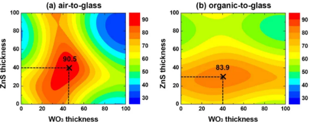
The dielectric-metal-dielectric (DMD) coating was initially developed for transparent heat reflection films because the DMD structure can be designed so that it has high transmission in the visible region and high reflection in the infrared region [9]. In these types of applications, what matters is the transmission of light from the air through the DMD films and the substrate to the air. With OLEDs, where the internal emission from the organic layer has to be outcoupled to air, it is organic-to-air transmission that is of interest. However, most previous works using DMD electrodes in OLEDs concern only the simple air-to-air transmittance of DMD films without considering the optical effect of organic media [4,10]. Calculation results comparing the air-to-glass transmittance Tair-to-glass and the organic-to-glass transmittance Torganic-to-glass values show a different trend. (i) First, the maximum Torganic-to-glass value that can
be achieved upon optimization is lower than the maximum Tair-to-glass value achievable with the
same DMD layers; (ii) secondly, variation in the thickness of the inner dielectric layer Di ( =
WO3 in the present case) result in little change in the transmittance in the organic-to-glass
case [See Fig. 2]. These findings mainly ensue because the index contrast between Di and
organic medium is much smaller than that between Di and air, making the optical effect of Di
less significant in terms of transmission/ reflection when the light is incident from an organic medium. Nevertheless, Fig. 2 shows that it is nonetheless possible to maximize Torganic-to-glass,
may be more important is the potential that the transmittance as well as other optical properties can be tuned in a relatively wide range to suit the different needs of various applications.
Fig. 2. Transmittance of a DMD structure upon variation of the thickness of the inner (WO3) and outer (ZnS) dielectric layers for a 15-nm-thick Ag layer: (a) air-to-glass vs. (b) organic-to-glass transmittance
3.2 Consideration of the microcavity / interference effect in DMD-based OLEDs
The presence of finite reflectance at DMD-organic interfaces and strong reflectance at organic-metal interfaces can result in a microcavity effect that is typically found in top-emitting OLEDs with a semitransparent thin metal electrode. By adopting the so-called Smith method, in which a DMD multilayer stack is effectively regarded as one single medium, as shown in Fig. 1(b) [11], the overall light output from a DMD-based OLED at a given wavelength λ will be proportional to I0(λ) × Gcav(λ), in which I0(λ) is the intensity of the light
generated inside the active layer by the emitter under no cavity effect, and Gcav(λ), the cavity
enhancement factor, is given by [12,13]:
cav( ) FP( ) TI( ; )0 G λ = f λ ×f λz (1) with
(
)
2 2 1 4 sin 2 DMD FP Al DMD Al DMD T f R R R R φ = ∆ − + (2)(
)
org org,EML Al Al 4 cos 1 2 cos o TI Al n z f R R φ π θ λ = + + − + (3)in which fFP(λ) and fTI(λ) are the Fabry-Perot factor and the two-beam interference factor,
respectively, z0 is the location of the emission zone measured from the organic/Al interface, TDMD is the transmittance through DMD films from the organic material (NPB in this work) to
the glass (or to air if DMD is used as the top electrode in a top-emission OLED), RAl and RDMD are the reflectance values at the organic-Al ( = A) and DMD-organic interfaces ( = B),
respectively. Additionally, ∆φ is the round-trip phase term given by Al DMD NPB,Alq3 4 i icos( )i i n d π θ φ φ φ λ = ∆ = − − +
∑
(4)in which φAl and φDMD are phase changes occurring upon reflections at interfaces A and B,
being NPB or Alq3. Reflection that can occur at the NPB/ Alq3 interface is ignored in the
above equations because the refractive index difference is small between NPB and Alq3. fTI(λ)
considers the effect of the interference between the two beams shown in Fig. 1(b); this value is common for all of the devices under study when one assumes that the emission zone is nearly identical among those devices.
4. Results and discussions
4.1 Optical effect of an inner dielectric layer
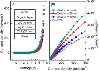
Figure 3 shows the current density-voltage (J-V) and luminance-current density (L-J) characteristics of OLED devices in a structure of glass/ X/ NPB (50nm)/ Alq3 (50nm)/ LiF
(1nm)/ Al with X being ITO or ZnS (30nm)/ Ag (15nm)/ WO3 (x nm) for x values of 5, 20,
and 30 nm. In Fig. 3(a), one can first note that the current density values of the ZAW-based devices do not show much variation in the range of WO3 thickness studied. The conductivity
of WO3 films prepared in the same way was found to be on the order of 10 −6
S/cm, similar to that of p-doped organic semiconductors [14]. This range of conductivity is large enough to make the voltage drop over the thickness of WO3 virtually negligible in the range of thickness
under study. The relatively high conductivity and large work function (4.7-6.4eV) of WO3
makes hole injection from Ag to WO3 and to NPB layer efficient, yielding a net current that is
comparable to that of ITO-based reference cells [15,16]. The important role of WO3 in a ZAW
structure as a hole injection layer was previously recognized by the authors in an experiment comparing the turn-on voltages of ZAW-based devices with those of devices based on ZnS/ Ag/ ZnS anodes [4,5].
Fig. 3. (a) Current density-voltage (J-V) and (b) luminance-current density (L-J) characteristics of OLED devices in a structure of glass/ X/ NPB (50nm)/ Alq3 (50nm)/ LiF (1nm)/Al, with X being ITO or ZnS (30nm) / Ag (15nm) / WO3 (x nm) for x values of 5, 20, and 30 nm. L was measured at a direction normal to the substrate.
In contrast to the case of the current density, the thickness of WO3 makes a clear
difference in the forward luminous efficiency (ηL) [See Fig. 3(b)]. Considering the
equivalence of the current density at a given voltage for all of the ZAW-based devices, it becomes clear that the observed difference in luminous efficiency comes mainly from an optical effect. Additionally, the device with the 5-nm-thick WO3 layer has a higher ηL value
compared to devices with a 20 or 30-nm-thick WO3 layer (See Table 1 for a summary). On the
other hand, the Torganic-to-glass value of the ZAW electrode with 5-nm-thick WO3 is lower than
those of ZAW electrodes with 20 or 30-nm-thick WO3 layers, as shown in Fig. 4(a) and
Table 1. It is important to note that previous works based on DMD electrodes were mostly concerned with achieving a high transmittance to obtain high-performance OLEDs. The results shown here, however, suggest that high transmittance may not always guarantee high
efficiency in DMD-based OLEDs. This is similar to what was observed in top-emitting OLEDs with a thin metal and an optical capping layer [17].
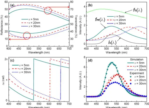
Figures 4(b) presents the fTI(λ), I0(λ), and fFP(λ) values of ZAW-based OLEDs for x values
of 5, 20, and 30 nm. This figure shows that the peak values for the Fabry-Perot resonance term fFP(λ) are quite different from device to device. What makes a difference depending on
the thickness of the WO3 is in fact the degree of matching between the peak of fFP(λ) and that
of I0(λ). As shown in Fig. 4(b), the peak wavelength for fFP(λ) shifts toward a longer
wavelength as WO3 becomes thicker; This is because the major reflection in ZAW electrodes
occurs at the Ag/ WO3 interface. That is, an increase in the WO3 thickness by ∆d will increase
the optical path length by 2nWO3 ∆d per round-trip, shifting φZAW and ∆φ accordingly [See Fig.
4(c)]. For the case of a device with 30-nm-thick WO3 layer, the Fabry-Perot resonance peak is
too far from that of the emission spectrum of Alq3, which makes its luminous efficiency
smaller than other ZAW-based devices. In case of the device with a 5-nm-thick WO3 layer,
however, the resonant wavelength matches well with the peak wavelength of the emission spectrum of Alq3 ; thus, it exhibits higher luminous efficiency compared to the other devices.
It is also noted that the mismatch between I0(λ) and fFP(λ) causes not only the emission
intensity to be reduced but also the emission spectrum to have a larger full-width at half-maximum (FWHM) [See Fig. 4(d) and Table 1].
Fig. 4. (a) Reflectance and transmittance, (b) fTI(λ), I0(λ), and fFP(λ), and (c) ∆φ of DMD-based OLEDs for WO3 thicknesses(x) of 5, 20, and 30 nm. (d) Comparison of the measured emission spectra I(λ) and the simulation result using Gcav(λ) × I0(λ) for DMD-based OLEDs. During the fitting procedure, the thickness of each layer was allowed to vary only within 10% from the nominal thickness.
It should also be noted that the peak location of fFP(λ) is not determined solely by the
cavity resonance condition; it is of course the major factor but the spectral dependence of
RZAW and TZAW can have some influence. For example, when x = 20 nm, the cavity resonant
condition, where the round-trip phase term is 2πm (m is integer), will be met at λ of 604 nm. However, for λ > 604 nm, RZAW increases with λ, enhancing the value of fFP(λ) in an
off-resonance condition, slightly shifting the peak location of fFP(λ) to 612 nm. Regarding the net
will be determined by all of the three factors: fTI(λ), I0(λ), and fFP(λ). In order to check the
validity of our descriptions, the experimental emission spectra of each case were fitted using
Gcav(λ) × I0(λ). During the fitting procedure, the thickness of each layer was allowed to vary
only within 10% from the nominal thickness. As for the overall magnitude, Gcav(λ) × I0(λ) was
scaled to match the peak value of I(λ) in each case. Figure 4(d) shows that Gcav(λ) × I0(λ) is in
good agreement with the actual emission spectra I(λ). In fact, scaling factors differed at most within 13% from case to case, indicating that the present optical analysis is also valid in terms of the relative magnitudes among different cases.
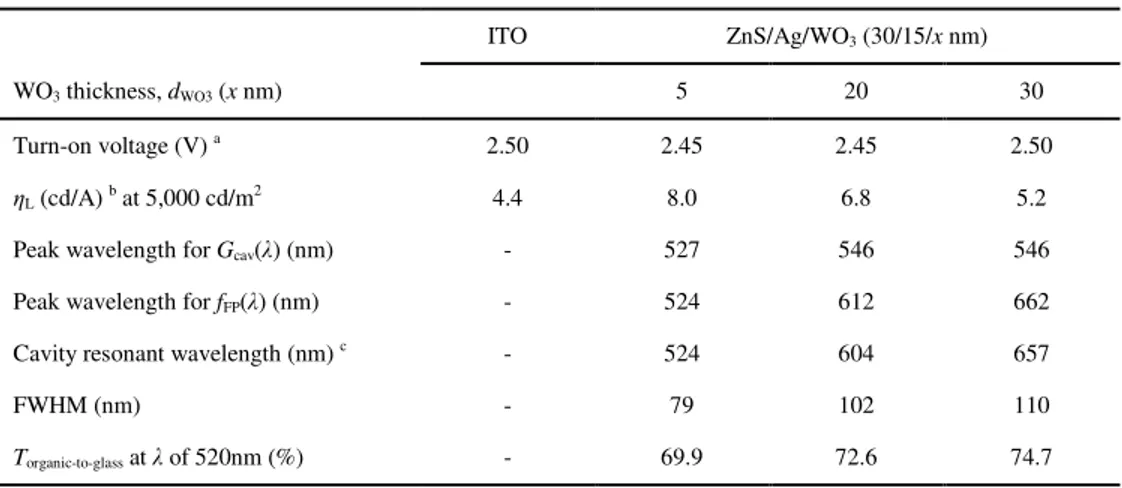
Table 1. Device Characteristics of ZAW-based OLEDs vs. the Thickness of the WO3
Layer
ITO ZnS/Ag/WO3 (30/15/x nm)
WO3 thickness, dWO3 (x nm) 5 20 30
Turn-on voltage (V) a 2.50 2.45 2.45 2.50
ηL (cd/A) b at 5,000 cd/m2 4.4 8.0 6.8 5.2
Peak wavelength for Gcav(λ) (nm) - 527 546 546
Peak wavelength for fFP(λ) (nm) - 524 612 662
Cavity resonant wavelength (nm) c - 524 604 657
FWHM (nm) - 79 102 110
Torganic-to-glass at λ of 520nm (%) - 69.9 72.6 74.7
a Voltage corresponding to L of 1 cd/m2. b measured at a direction normal to the substrate. c ∆φ = 2πm, m: integer.
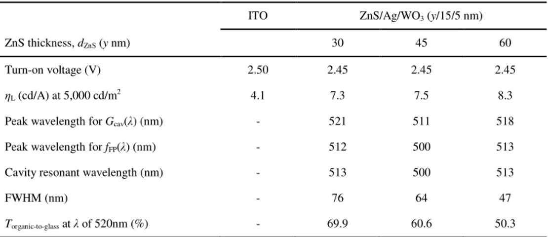
4.2 Optical effect of the outer dielectric layer
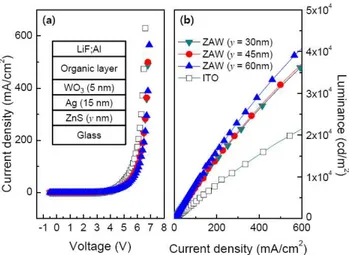
Figure 5 shows the J-V and L-J characteristics of OLED devices in a structure of glass/ Y/ NPB (50nm)/ Alq3 (50nm)/ LiF (1 nm)/Al, with Y being ITO or ZnS (y nm) / Ag (15nm) /
WO3 (5 nm) for y values of 30, 45, and 60 nm. As summarized in Table 2, all of the
ZAW-based OLEDs exhibit much higher ηL values compared to the ITO-based devices. For a y
value of 60 nm, the improvement ratio of ηL with respect to that of ITO-based devices was as
large as 2.
The optical analysis presented in Figs. 6(a) and 6(b) reveals that the improvement in this case is a combined effect of an enhanced cavity effect and its good spectral overlap with the emission spectrum of Alq3. Recall that TZAW and RZAW tend to vary more sensitively
depending on the thickness of ZnS ( = dZnS) than on the WO3 thickness ( = dWO3) due to a
relatively high index contrast at the ZnS/ glass interface [See Fig. 2(b)]. While RZAW may
increase or decrease with dZnS, the results presented in Fig. 6(b) indicate that RZAW increases
with dZnS for the range of thickness studied in this work. On the other hand, the net round-trip
phase change ∆φ remains nearly identical as dZnS varies [Fig. 6(c)], showing a good contrast
with the previous case of dWO3 variation. The thickness of WO3 being fixed at 5 nm, which
was previously shown to be near the phase resonance condition at λ ≈520 nm, all three types of devices meet the resonant condition near the peak wavelength of I0(λ). Thus, fFP(λ) shows a
good spectral overlap with I0(λ) in each case. Together with the high degree of spectral
overlap, the increase in RZAW with dZnS results in an enhancement in fFP(λ). This combined
Fig. 5. (a) Current density-voltage (J-V) and (b) luminance-current density (L-J) characteristics of OLED devices in a structure of glass/ Y/ NPB (50nm)/ Alq3 (50nm)/ LiF (1 nm)/Al, with Y being ITO or ZnS (y nm) / Ag (15nm) / WO3 (5 nm) for y values of 30, 45, and 60 nm.
Fig. 6. (a) Reflectance and transmittance, (b) fTI(λ), I0(λ), and fFP(λ), and (c) ∆φ of DMD-based OLEDs for ZnS thicknesses(y) of 30, 45, and 60 nm. (d) Comparison of the measured emission spectra I(λ) and the simulated emission spectra Gcav(λ) × I0(λ) of DMD-based OLEDs. The fitting procedures for (d) are identical to those used in Fig. 4(d).
The emission spectra of these ZAW-based OLEDs, which exhibit a good fit to the calculated Gcav(λ) × I0(λ) values [Fig. 6(d)], indeed exhibit much less variation in the peak
emission wavelength, which is consistent with the explanation given above. In addition, there is a decrease in their FWHM values with the increase in dZnS. This is mainly because the
Table 2. Device Characteristics of ZAW-based OLEDs vs. the Thickness of the ZnS Layer
ITO ZnS/Ag/WO3 (y/15/5 nm)
ZnS thickness, dZnS (y nm) 30 45 60
Turn-on voltage (V) 2.50 2.45 2.45 2.45
ηL (cd/A) at 5,000 cd/m2 4.1 7.3 7.5 8.3
Peak wavelength for Gcav(λ) (nm) - 521 511 518
Peak wavelength for fFP(λ) (nm) - 512 500 513
Cavity resonant wavelength (nm) - 513 500 513
FWHM (nm) - 76 64 47
Torganic-to-glass at λ of 520nm (%) - 69.9 60.6 50.3
4.3 Effect on angular emission characteristics
Devices with a thicker inner dielectric layers dDi, within the range of thickness tried in this
study, turned out to have characteristics that are closer to those of Lambertian light source as shown in Figs. 7(a) and 7(b). It was noted that in devices where the cavity resonance wavelength λRES of fFP(λ) matches the peak wavelength λAlq3 of the Alq3 emission spectrum
forθ of 0°, the emission will in fact be more intense in a forward (normal) direction than in an off-normal direction because the resonance enhancement will be subdued in the off-normal direction. This is the case presented in Fig. 7(b). For devices with thicker WO3 layers,
however, λRES is larger than λAlq3 when θ = 0°. As θ increases, their λRES values will become
smaller, as they scales with cos θ, and will become matched better to λAlq3, enhancing the
emission from a side-viewing angle. This enhancement in the off-normal direction, together with the relatively weak cavity effect due to small RZAW values of the devices with the thicker dWO3, is likely to make the overall emission of DMD-based OLEDs closer to that of the
Lambertian source.
Fig. 7. Angular emission characteristics of OLED devices in a structure of glass/ ZAW/ NPB (50nm)/ Alq3 (50nm)/ LiF (1nm)/Al, with ZAW being (a) ZnS (30nm) / Ag (15nm) / WO3 (x nm) for x values of 5, 20, and 30 nm and (b) ZnS (y nm)/ Ag (15nm)/ WO3 (5 nm) for y values of 30, 45, and 60 nm
4.4 Summary: application-specific optimization of the DMD structure
As shown in the previous section, the optical effect of each layer in a DMD structure is different and its optimization should consider not only transmission but also the overall cavity structure and its correlation with the emission spectrum of emitter molecules. Furthermore, the optimization process should consider the balance between luminous efficiency and the angular and/or spectral characteristics according to the needs of the target application. While
higher luminous efficiency will always be desired, the preference for a specific pattern of angular or spectral dependency over others varies depending on the application of interest. In display applications, for example, light sources are desired to have a narrow spectral width to allow for a large color gamut; in lighting applications, on the other hand, color rendering close to natural sunlight will generally prefer a broad spectral distribution. In some applications such as a small display in a personal portable electronic device, a narrow viewing angle is often tolerated or even preferred, whereas a large display such as TV will generally prefer a wide viewing angle.
For applications in which high luminous efficiency in a forward direction is preferred, the thickness of the inner dielectric layer dDi should be determined first to match the cavity
resonance wavelength λRES (θ = 0°) to the peak emission wavelength λEML of the emitter. The
thickness of the outer dielectric layer dDo should then be chosen depending on the target
requirements: a stronger forward luminance and narrower spectral width will require a dDo
value that can lead to a high RDMD; if stronger forward luminance is preferred but a narrow
spectral width is not, dDo leading to a high TDMD value may be chosen.
For applications that require Lambertian-like emission with a less spectral dependence and/or a broad spectral width, the value of dDi may be chosen such that λRES (θ = 0°)
mismatches λEML on purpose. Additionally, dDo may be chosen such that a high TDMD value is
achieved to reduce the cavity effect. It is important to note, however, that even a configuration leading to a high TDMD value at a certain wavelength may have a relatively large RDMD value in
other wavelengths due to the spectral dependence of the DMD structure. Therefore, it is necessary to monitor the overall distribution of Gcav(λ;θ) × I0(λ) carefully to predict the net
emission spectra. By changing λRES (θ = 0°) so that it is larger or smaller than λEML, the overall
color temperature of the emission spectrum may be tuned as well.
For applications in which the total optical power output is a main concern, dDi and dDo
should be chosen so that the integration of Gcav(λ;θ) × I0(λ) over the wavelength and emission
angle is maximized. In all of the cases noted here, dDi should be within a certain limit so that
the desired injection properties may not be compromised. One may also need to be reminded that the photons propagating with large emission angle (with respect to the vertical direction) will also be subject to the waveguiding effect that is found in ITO-based OLEDs. Eventual improvement may then need to include the strategies overcoming those effects. See the work by Lim et al. for example [18].
It has to be noted throughout the article that the validity of optical analysis in this study relies on the assumption that participating layers are optically flat; this is a good approximation in most cases, but attention must be paid to the very thin layers. For example, 5-nm-thick WO3 films may be too thin to be regarded continuous. WO3 having the optical
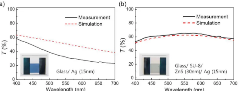
constants that are very similar to those of organic layers, however, its optical effect in terms of reflection/transmission at associated interfaces would be small. Although it can have some influence through the optical cavity effect as discussed in 4.1, the continuity of the 5-nm-thick thin WO3 film would not be that critical in optical analysis because it takes up only ~5% of
the total cavity length. In case of an Ag film, however, its film morphology was shown to get influenced by the roughness or the adhesion compatibility of an underlying layer [5]. Note that the film morphology of Ag films can be critical because formation of an island-like morphology instead of continuous one can result in a high sheet resistance. Furthermore, an Ag film with such “disconnected” morphology can absorb more photons in the visible spectral range and thus can become a loss mechanism for photons that need to be outcoupled. This is regarded due to the surface Plasmon effect typical of Ag-nanoparticles which results in an enhancement in absorption in the visible spectral range [19]. For the same reason, the transmittance of a single- or multilayer stack containing an Ag film with the “disconnected” morphology cannot be fitted to the modeling results based on the optical constants known for Ag thin films [8] [See Fig. 8(a)]. In contrast, Ag films used in this study had a relatively continuous morphology [5], and so the transmittance of multilayer stacks containing them were modeled very well with the reported optical constants for thin-film Ag [8] [Fig. 8(b)], supporting the validity of the present work.
Fig. 8. Measured (solid) and simulated (dashed) transmittance (T) spectra of (a) glass/ Ag (15nm) and (b) glass/SU-8/ ZnS (30nm)/Ag (15nm) samples. Inset: the photographs of the respective samples. The Ag film grown on a bare glass shown in (a) has an island-like morphology.
4. Conclusions
This study investigated the optical properties of organic light-emitting diodes (OLEDs) based on dielectric-metal-dielectric (DMD) transparent electrodes, which have advantages over conventional transparent conductive oxides (TCOs) particularly in terms of their high mechanical flexibility, low sheet resistance, and applicability as a damage-free top electrode. This study indicates that the optical characteristics of DMD-based OLEDs can be widely tuned through careful control of the interplay between the microcavity effect and the transmittance of DMD electrodes and their correlation with the emission spectrum of the emitting molecule. Different optical effects of inner and outer dielectric layers were identified in a joint experimental and theoretical study, and optimization strategies suitable for various applications were discussed. Upon variation of the DMD structure, efficient OLEDs with forward luminous efficiency twice as large as that of ITO-based reference cells were demonstrated along with OLEDs having near-Lambertian emission with luminous efficiency comparable to that of ITO-based reference cells. While the Ag-based DMD electrodes may have a material cost similar to that of ITO electrodes, those based on Cu are expected to have a significantly lower material cost; Although Cu-based DMDs may have a slightly lower performance due to absorption in the visible range, such cost benefit would be critical in applications such as lighting or low-end displays, which typically have stringent cost requirements. The work presented here will likely lay the foundation for the full utilization of the benefits that DMD electrodes can offer to OLEDs in both displays and lighting applications
Acknowledgments
This work was supported by Basic Science Research Program through the National Research Foundation of Korea (NRF) funded by the Ministry of Education, Science and Technology (No. R11-2007-045-01001-0), and by the Ministry of Knowledge Economy (MKE) and Korea Institute for Advancement in Technology (KIAT) through the Workforce Development Program in Strategic Technology.