1. Introduction
Recently, molecular diagnosis, which
accurately diagnoses genetic diseases or pathogenic diseases at the molecular level,
This research was supported by Kumoh National Institute of Technology (2017-104-052).
* R&D Center, Leo LSI
** Corresponding Author : School of Electronic Engineering, Kumoh National Institute of Technology (jimin.cheon@ku moh.ac.kr)
Received January 14, 2020 Revised January 29, 2020 Accepted January 30, 2020
A Single-Bit 2nd-Order Delta-Sigma Modulator with 10-μm Column-Pitch for a Low Noise CMOS Image Sensor
Min-Woo Kwon* and Jimin Cheon**
저잡음 CMOS 이미지 센서를 위한 10μm 컬럼 폭을 가지는 단일 비트 2차 델타 시그마 모듈레이터
권 민 우*, 천 지 민**
Abstract In this paper, a single-bit 2nd-order delta-sigma modulator with the architecture of cascaded-of-integrator feedforward (CIFF) is proposed for column-parallel analog-to-digital converter (ADC) array used in a low noise CMOS image sensor. The proposed modulator implements two switched capacitor integrators and a single-bit comparator within only 10-μm column-pitch for column-parallel ADC array. Also, peripheral circuits for driving all column modulators include a non-overlapping clock generator and a bias circuit. The proposed delta-sigma modulator has been implemented in a 110-nm CMOS process. It achieves 88.1-dB signal-to-noise-and-distortion ratio (SNDR), 88.6-dB spurious-free dynamic range (SFDR), and 14.3-bit effective-number-of-bits (ENOB) with an oversampling ratio (OSR) of 418 for 12-kHz bandwidth. The area and power consumption of the delta-sigma modulator are 970⨯10 μm2 and 248 μW, respectively.
요 약 본 논문에서는 polymerase chain reaction (PCR) 응용에 적합한 저잡음 CMOS 이미지 센서에 사용되는 컬럼-패러럴 analog-to-digital converter (ADC) 어레이를 위한 cascaded-of-integrator feedforward (CIFF) 구 조의 단일 비트 2차 델타-시그마 모듈레이터를 제안하였다. 제안된 모듈레이터는 CMOS 이미지 센서에 입사된 빛의 신 호에 해당하는 픽셀 출력 전압을 디지털 신호로 변환시키는 컬럼-패러럴 ADC 어레이를 위해 하나의 픽셀 폭과 동일한 10μm 컬럼 폭 내에 2개의 스위치드 커패시터 적분기와 단일 비트 비교기로 구현하였다. 또한, 모든 컬럼의 모듈레이터 를 동시에 구동하기 위한 주변 회로인 비중첩 클록 발생기 및 바이어스 회로를 구성하였다. 제안된 델타-시그마 모듈레 이터는 110nm CMOS 공정으로 구현하였으며 12kHz 대역폭에 대해 418의 oversampling ratio (OSR)로 88.1dB의 signal-to-noise-and-distortion ratio (SNDR), 88.6dB의 spurious-free dynamic range (SFDR) 및 14.3비트 의 effective-number-of-bits (ENOB)을 달성하였다. 델타 시그마 모듈레이터의 면적 및 전력 소비는 각각 970⨯10 μm2 및 248μW이다.
Key Words : Analog-to-digital converter, CIFF, CMOS image sensor, column-parallel ADC array,
delta-sigma modulator
is revolutionizing the field of medical technology. There are many techniques used for molecular diagnosis, but the representative one is polymerase chain reaction (PCR) [1, 2].
The optical PCR biosensor is a measurement technology capable of real-time detection of a target material based on high selectivity and sensitivity [3].
The optical PCR biosensor includes a light source for generating light and a light detector for detecting spectro-chemical characteristics of the material.
In particular, a low noise CMOS image sensor (CIS) used as an optical detector is needed because it must be able to detect extremely dim light. Since the analog-to-digital converter (ADC) for the low noise CIS requires more than 13-bit resolution [4], a commercial CIS implemented with column-parallel single-slope ADC array with 10~12 bits of resolution cannot be used for the PCR application. Typically, a low noise, high resolution ADC are implemented with a delta-sigma ADC. The delta-sigma ADC can achieve high signal to noise ratio (SNR) within the signal band by effectively suppressing quantization noise with oversampling and noise shaping techniques [5].
When the delta-sigma ADC structure are employed in a CIS with a column-parallel ADC array, the most difficult thing is to place the comparator and switched capacitor integrators that make up the high-resolution delta-sigma modulator in the same column-pitch as the pixel-pitch [6].
In this paper, we propose a delta-sigma modulator with 10-μm column-pitch for low noise CIS with column-parallel ADC
structure used in PCR applications. In particular, we propose a design that can be implemented as a column parallel delta-sigma modulator structure so that the analog signal detected by the photodiode can be converted into a high resolution digital signal and read out more quickly.
2. Proposed Single-Bit 2nd-Order Delta-Sigma Modulator
2.1 Architecture
In the general feedback delta-sigma modulator, since both the input signal and the output signal of the integrator are functions of the input signal, the slew occurs in the amplifier when a large input signal is applied, and the signal is distorted due to the large integrator output signal. Therefore, to avoid these, accepting only a small input signal increases the power consumption because the SNR is reduced and the noise of the amplifier must be reduced. When the integrator output range is increased, the rate of change of the voltage gain according to the signal magnitude increases, which causes distortion of the signal. To avoid this, high voltage gain of the amplifiers in the integrator is required. In design conditions where low supply voltage and low power dissipation must be met, it is very difficult to design the amplifier to satisfy both the high voltage gain and the wide output range of the amplifier. Therefore, the feedforward delta-sigma modulator structure is used instead of the feedback delta-sigma modulator structure to solve these problems at low power supply conditions [7-9].
The single-bit structure of the delta-sigma modulator structure is simpler than the multi-bit structure, thereby reducing the design burden of the entire circuit. In addition, the single-bit architecture has the advantage of minimizing the non-ideal characteristics of the fully differential amplifier, switches, and capacitors used in the integrator [10, 11].
Fig. 1 shows the block diagram for the behavioral simulation of the proposed single-bit 2nd-order delta-sigma modulator using cascaded of integrator feedfoward (CIFF) structure. The transfer function of the 2nd-order structure can be expressed as follows.
(1)Note that z is a complex number for z-transform. At the output Y, the input X appears without delay, and the quantization noise E is represented as passing through the 2nd-order high pass filter. In this case, the outputs of the integrators I1 and I2 are derived as follows.
(2)
(3)From equation (2) and equation (3), it can be known that I1 and I2 are independent of the magnitude of X, so if E is kept at a low level, they can generate stable outputs regardless of the magnitude of X.
When the single-bit quantizer is used, the
Y(z)
X(z) z
-11-z
-1z
-11-z
-11
1 1
2
1
I
1(z) I
2(z)
DAC
Fig. 1. Block diagram for the behavioral simulation of the single-bit 2nd-order CIFF delta-sigma modulator
Y(z)
X(z) z
-11-z
-1z
-11-z
-11/3
1/5 1/3
2/3
1
I
1(z) I
2(z)
DAC
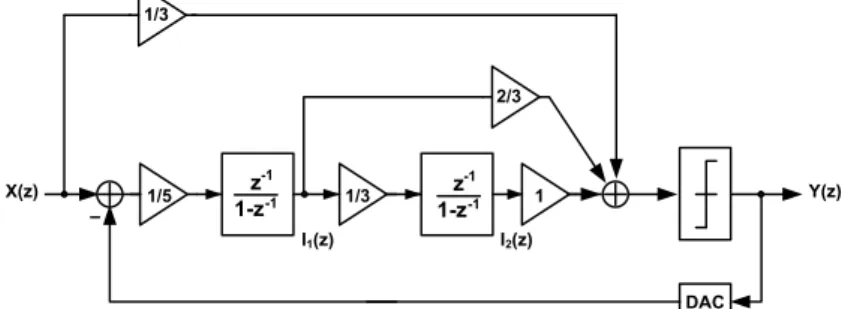
Fig. 2. Block diagram for the behavioral simulation of the proposed single-bit 2nd-order CIFF delta-sigma modulator
with the loop filter’s coefficients adjusted to meet stability and operation voltage range of the integrators
output range of the integrators must be reduced to satisfy the loop filter stability and to be implemented within the power supply range [8]. Fig. 2 shows the block diagram of the single-bit 2nd-order CIFF delta-sigma modulator with the loop filter's coefficients adjusted to meet these conditions. When the coefficients are adjusted as shown in Fig. 2, the histogram of the output of the first integrator, which is obtained by the behavioral simulation, can be seen that it is maintained within about 33% of the power supply voltage as shown in Fig. 3. This characteristic is maintained even when the input signal is increased by –6 dB relative to the power supply voltage.
Fig. 3. Histogram of the output of the first integrator
In addition, the DC voltage gain of the operational transconductance amplifier (OTA) used in each integrator can be obtained as shown in Table 1 through behavioral simulation. According to Table 1, it can be seen that when the OTAs of all integrators have a DC voltage gain of 60 dB or more, the SNR can be similar to that of using ideal OTAs.
Table 1. SNR and ENOB according to DC voltage gain of each stage in the proposed delta-sigma modulator
1
st2
ndSNR ENOB
Ideal Ideal 108.7 dB 17.76-bit 80 dB 80 dB 108.4 dB 17.71-bit 80 dB 60 dB 111.1 dB 18.16-bit 80 dB 40 dB 101.2 dB 16.5-bit 80 dB 20 dB 87.26 dB 14.2-bit 60 dB 80 dB 109.9 dB 17.96-bit 60 dB 60 dB 108.5 dB 17.73-bit 60 dB 40 dB 101.8 dB 16.62-bit 60 dB 20 dB 81.84 dB 13.3-bit 40 dB 40 dB 94 dB 15.32-bit 40 dB 20 dB 76.32 dB 12.38-bit 20 dB 20 dB 66.78 dB 10.8-bit
Fig. 4. Circuit diagram of the proposed single-bit 2nd-order CIFF delta-sigma modulator
2.2 Circuit Implementation
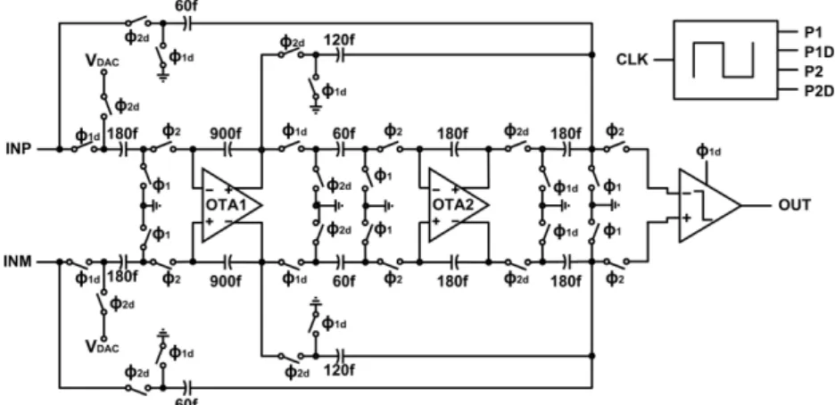
The proposed delta-sigma modulator has a single-bit 2nd-order CIFF structure as shown in Fig. 4 to achieve high resolution. The proposed circuit consists of two switched-capacitor integrators using OTAs, a clock generator that generates non-overlapping clocks for stable sample-and-hold operation and integration operation, a single bit comparator, and other logic for control and digital signal output.
2.2.1 OTA for integrators of 1st/2nd-stage Due to the characteristics of the CIFF structure, the output swing range of the integrators is small, so the folded cascode OTA structure is used to easily obtain DC voltage gain of 60 dB or more while
securing phase margin for stability [12].
The OTA used in the integrators shown in Fig. 5(a) is a fully differential structure and uses a PMOS input to reduce noise. Fig.
5(b) shows a common mode feedback (CMFB) circuit used to stabilize the output common mode of a fully differential OTA.
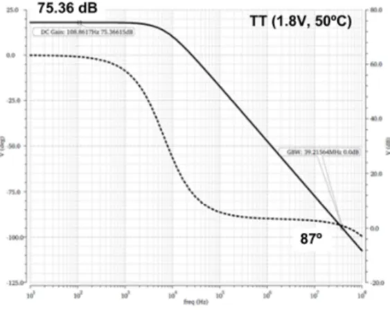
Fig. 6. Frequency response obtained by performing the post-simulation with parasitic effects on the OTA for the integrators
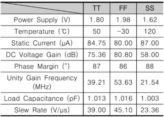
Fig. 6 shows the frequency response obtained by performing the post-simulation with parasitic effects on the OTA for the integrators. The simulation was performed under normal process (TT), temperature (5 0℃), and voltage conditions (1.8-V power supply), with 75.36-dB DC voltage gain, 87-degree phase margin, and 39.21-MHz unity gain frequency. Table 2 shows the corner post-simulation results of the OTA.
(a)
(b)
Fig. 5. OTA for the integrators of 1st-/2nd-stage (a)
PMOS input folded cascode OTA circuit (b) dynamic
CMFB circuit
Table 2. Corner post-simulation results of the OTA
TT FF SS
Power Supply (V) 1.80 1.98 1.62
Temperature (℃) 50 -30 120
Static Current (μA) 84.75 80.00 87.00 DC Voltage Gain (dB) 75.36 80.80 58.00
Phase Margin (°) 87 86 88
Unity Gain Frequency
(MHz) 39.21 53.63 21.54
Load Capacitance (pF) 1.013 1.016 1.003 Slew Rate (V/μs) 39.00 45.10 23.36
2.2.2 Single-bit comparator
Fig. 7. Dynamic regenerative comparator
Operating characteristics of the comparator used in this paper may be relatively less precise. This is because the nonlinearities of the comparators are already noise-shaped by the loop filter.
Therefore, instead of using the comparator including the pre-amplifier and offset cancellation circuit of [13], a simple dynamic regenerative comparator is used as shown in Fig. 7. The comparator consists of a dynamic latch that consumes low power and operates as follows. When the clock
CLK goes logically low, the latch is reset, and both the VOP and VON outputs of the comparator go logically high. When the clock CLK becomes logically high, the latch will perform a regeneration operation.
2.2.3 Non-overlapping clock generator Fig. 8 shows a clock generator for generating non-overlapping clocks [14]. The clock generator basically forms a feedback circuit with two NAND gates, and a delay circuit consisting of multiple inverters is connected to each NAND output. The inverters in the feedback loop can be used to adjust clock delay and non-overlapping intervals. The clock generator uses the input clock (CLK) to generate clock signals P1 and P2. In addition, the delayed clock signals P1D and P2D are generated from P1 and P2 to implement the bottom-plate sampling technique that can avoid charge injection from the switches [15].
Fig. 8. Circuit diagram of the clock generator for non-overlapping clocks
3. Experimental Results
Fig. 9 shows the microphotograph of the fabricated chip with 4 delta-sigma modulators. The proposed single-bit 2nd-order CIFF delta-sigma modulator uses 1.8V supply voltage and is fabricated in 1-poly 8-metal 110-nm CMOS process. A
delta-sigma modulator has an area of 970⨯
10 μm2 and power consumption of 248 μW.
Fig. 9. Microphotograph of the proposed delta-sigma modulator chip
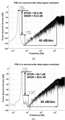
Fig. 10 shows the spectral analysis of the output signal of the proposed delta-sigma modulator obtained with pre-simulation on a circuit whose parasitic components are not considered and post-simulation on a circuit whose parasitic components are extracted from the layout, respectively.
With an oversampling ratio (OSR) of 418 and an input signal of 4 kHz for 12-kHz bandwidth, the post-simulation results show 88.1-dB signal to noise and distortion ratio (SNDR), 88.6-dB spurious free dynamic range (SFDR), and 14.3-bit effective number of bits (ENOB), while the pre-simulation results show 95.0-dB SNDR, 93.8-dB SFDR, and 15.3-bit ENOB. This is a performance degradation due to the layout of the modulator on a 10-μm column-pitch.
Layout of the circuit in a 10-μm column-pitch introduces difficulties in circuit placement and signal connection, which increases mismatch between transistors and capacitors. In addition, since each device is laid out in close proximity, parasitic components increase and crosstalks between signals increase.
Table 3 shows the characteristics of the implemented single-bit 2nd-order delta-sigma
modulator.
(a)
(b)
Fig. 10. Spectral analysis of the output signal of the proposed delta-sigma modulator (a) pre-simulation result (b) post-simulation result
Table 3. Characteristics of the implemented single-bit 2nd-order delta-sigma modulator
Parameters Contents
Process 110-nm CMOS
Power Supply (V) 1.8
OSR 418
Sampling Frequency (MHz) 10
SNDR (dB) 88.1
SFDR (dB) 88.6
Area (μm
2) 970⨯10
Power Consumption (μW) 248
4. Conclusion
We proposed the delta-sigma modulator with 10-μm column-pitch for low noise CIS with column-parallel ADC structure used in PCR applications. It implements two switched capacitor integrators and a single-bit comparator within only 10-μm column-pitch for column-parallel ADC array. The proposed delta-sigma modulator has been implemented in a 110-nm CMOS process. It achieves 88.1-dB SNDR, 88.6-dB SFDR, and 14.3-bit ENOB with OSR of 418 for 12-kHz bandwidth. The area and power consumption of the delta-sigma modulator are 970⨯10 μm2 and 248 μW, respectively.
REFERENCES
[1] C. Zhang and D. Xing, “Miniaturized PCR Chips for Nucleic Acid Amplification and Analysis: Latest Advances and Future Trends”, Nucleic Acids Res., vol. 35, no. 13, 2007.
[2] A. Hassibi, “CMOS Biochips for Point-of-care Molecular Diagnostics”, Hot Chips, 2014.
[3] A. Hassibi, R. Singh, A. Manickam, R.
Sinha, B. Kuimelis, S. Bolouki, P.
Naraghi-Arani, K. Johnson, M. McDermott, N. Wood, P. Savalia, and N. Gamini, "A fully integrated CMOS fluorescence biochip for multiplex polymerase chain-reaction (PCR) processes", Proc. IEEE Int. Solid-State Circuits Conf., pp. 68-69, 2017.
[4] H. Eltoukhy, K. Salama, and A. Gamal, "A 0.18- μm CMOS Bioluminescence Detection Lab-on-Chip", IEEE J. Solid-State Circuits, vol. 41, no. 3, pp. 651-662, Mar. 2006.
[5] S. Pavan, R. Schreier, and G. C. Temes, Understanding Delta-Sigma Data Converters, NJ, Piscataway:IEEE Press/Wiley, 2017.
[6] Y. Chae, J. Cheon, S. Lim, M. Kwon, K.
Yoo, W. Jung, D.-H. Lee, S. Ham, G. Han,
"A 2.1 Mpixel 120 frame/s CMOS image sensor with column-parallel △Σ ADC architecture", IEEE J. Solid-State Circuits, vol. 46, no. 1, pp. 236-247, Jan. 2011.
[7] K. Nam, S-M, Lee, D. K. Su and B. A.
Wooley, "A low-voltage low-power sigma-delta modulator for broadband analog-to-digital conversion", IEEE J.
Solid-State Circuits, vol. 40, no. 9, pp.
1855-1864, Sep. 2005.
[8] G. Ahn, D. Chang, M. Brown, N. Ozaki, H.
Youra, K. Yamamura, K. Hamashita, K.
Takasuka, G. C. Temes and U. Moon, "A 0.6-V 82-dB delta-sigma audio ADC using switched-RC integrators", IEEE J. Solid-State Circuits, vol. 40, no. 12, pp. 2398-2407, Dec. 2005.
[9] Y. Chae, I. Lee, and G. Han, "A 0.7 V 36 μ W 85 dB DR Audio △Σ Modulator Using Class-C Inverter", Proc. IEEE Int. Solid-State Circuits Conf., pp. 490-491, 2008.
[10] J. M. de la Rosa, R. del Río, CMOS Sigma-Delta Converters: Practical Design Guide, NJ, Hoboken:Wiley-IEEE Press, 2013.
[11] J. Roh, S. Byun, Y. Choi, H. Roh, Y.-G.
Kim, and J.-K. Kee, "A 0.9-V 60-μW 1-bit fourth-order delta-sigma modulator with 83-dB dynamic range", IEEE J. Solid-State Circuits, vol. 43, no. 2, pp. 361-370, Feb.
2008.
[12] D. A. Johns and K. Martin, Analog Integrated Circuit Design, New York:Wiley, 1997.
[13] Y. Geerts, M. Steyaert, and W. Sansen, Design of Multi-Bit Delta-Sigma A/D Converters, MA, Norwell:Kluwer, 2002.
[14] R. J. Baker, CMOS Mixed-Signal Circuit Design, New York:IEEE Press, 2002.
[15] R. Schreier, J. Silva, J. Steensgaard, and G.
C. Temes, "Design-oriented estimation of thermal noise in switched-capacitor circuits", IEEE Trans. Circuits Syst. I: Reg.
Papers, vol. 52, no. 11, pp. 2358-2368,
Nov. 2005.
Author Biography
권 민 우 (Min-Woo Kwon) [정회원]
⦁2016년 2월 : 금오공과대학교 전 자공학부 (공학사)
⦁2018년 2월 : 금오공과대학교 전 자공학과 (공학석사)
⦁2018년 3월 ~ 현재 : Leo LSI R&D Center 연구원
<관심분야> Delta-Sigma ADC
천 지 민 (Jimin Cheon) [종신회원]