I. Introduction
Galois Fields have largely been applied in the error control codes, crytographic system, and switching system[1]. Important operations in Galois Fields are addition, multiplication, division, and inversion. If field elements are represented in a
* 仁荷大學校 電子工學科
(Dept. of. Elec. Eng., Inha Univ.
** 가톨릭 大學校 情報通信電子工學部
(School. of. Info., Comm. & Elec. Eng., Catholic Univ.)
接受日:2004年 2月 24日, 修正完了日:2004年 7月 9日
Design of GF(3
m) Current-mode CMOS Multiplier
GF(3
m)상의 전류모드 CMOS 승산기 설계
Gi-Soo Na*, Gi-Young Byun**, Heung-Soo Kim* 羅 基 秀*, 卞 基 寧**, 金 興 壽*
Abstract
In this paper, we discuss on the design of a current mode CMOS multiplier circuit over GF(3m). Using the standard basis, we show the variation of vector representation of multiplicand by multiplying primitive element α, which completes the multiplicative process. For the GF(3m) multiplicative circuit design, we design GF(3) adder and multiplier circuit using current mode CMOS technology and get the simulation results. Using the basic gates - GF(3) adder and multiplier, we build the GF(3m) multiplier circuit and show the examples for the case m=3.
We also propose the assembly of the operation blocks for a complete GF(3m) multiplier. Therefore, the proposed circuit is easily extensible to other p and m values over GF(pm) and has advantages for VLSI implementation. We verify the validity of the proposed circuit by functional simulations and the results are provided.
Key-word : MVL, GF(pm), Current-mode, Ternary, DTOM
요 약
본 논문에서는 GF(3m)상의 전류모드CMOS 승산기의 설계에 관하여 논의한다. 피 승산항에 원시원소 α를 곱함으
로써 나타나는 피 승산항의 변화를 표준기저 표현을 이용하여 수식으로 전개하였다. GF(3m) 승산 회로를 구성하
기 위하여 전류모드 CMOS를 사용하여 GF(3)상의 가산기와 승산기를 설계하였고 시뮬레이션 결과를 보였다. 기 본 게이트들을 이용하여 GF(3m) 승산기를 설계하였고 m=3인 경우에 대하여 예를 보였다.
본 논문에서 제안한승산회로는 그 구성이 블록의 형태로 이루어지므로 GF(pm) 상에서 p와 m에 대한 확장이 용 이하며, VLSI 구현에 유리하다 할 수 있다. 본 논문에서 제안한승산회로를 타 승산회로와 비교하였고, 개선효과를 확인하였다.
standard basis form, then addition can be implemented with a simple circuit. But the other operations are much more complex. The study focuses on the hardware implementation of the fastand low-complexity multiplier over Galois Fields have been proposed.
In 1971, B.A. Laws[2] showed a cellular array multiplier over GF(2m). Since then, many multipliers have been proposed. C.S. Yeh[3], Massey-Omura[4], C.C. Wang[5], and many researchers showed many works of their own[6-7]. The previous binary logic circuits in GF(2m) have many advantages such as an efficientand easy design, layout and high packing density. But recently, an increase of interconnections has been a serious problem for a binary LSI[8,9]. As a solution of this problem, multiple-valued LSI has been expected since1970. In Multiple Valued Logic(MVL) system, many discrete logic levels can be defined but not confined to binary values. It is possible to increase the information content of the digital signals in logic circuits to higher value than binary circuits.
Therefore, the MVL circuits might solve the interconnection com-plexity, high speed, high packing density and low power dissipation.
For these reasons, many works have been studied about multiple-valued logic function realization. In 1981, the first commercially available circuits, in the form of a four valued read only memory(ROM) were shown[10]. After this, the multiple valued VLSI has attracted great interest in recent years as one of the most promising approaches for reducing the inter-connection complexity. In 1993, N. Kamiura[11]
showed a multiple valued cellular array circuits using CMOS. In 1997, T. Hanyu[12] showed a low power multiple valued current mode integrated circuit with current source control. In 1999, Y.
Hata[13] showed a multiple valued programmable logic array with unary function generators. In 2000, Seong[14]proposed MVL ALU using current-mode CMOS over GF(3m). Seong et al implemented the multiplication between two elements and the addition to need to irreducible polynomial arithmetic as a switch using proposed arithmetic cell.
Current-mode CMOS circuits have the compatibility for the requirements of VLSI design, and enable on low supply voltages with stable. The most important of these are the case of summation of signals and the difficulty in distribution of signals caused by the fan-out being equal to one.
In this paper, the new multiplier circuit using the standard basis over GF(3m) was proposed. Proposed GF(3m) multiplier circuit is composed of parallel operation structure about each modules and has the property of high speed because memory components wasn't used. As an example, we have designed the multiplier circuit over GF(33) and checked the behavior of the designed circuit by simulation tool.
This paper is organized as follows. In Section II, we summarize multiplication theory in GF(3m). This algorithm is mapping the hardware design in Section III. In addition, we provide a ternary adder and aternary multiplier, and symbolize them, and design GF(3) adder and multiplier circuit using current mode CMOS technology and get the simulation results. In Section IV, we show the circuit design of high parallel multiplier using digit transition operating module(DTOM). Finally, comparisons and conclusions are drawn in Section V.
II. Multiplication over GF(pm)
Prior to discussing the newly proposed design method in this paper, it is believed that a brief discussion of Galois fields would be helpful.
More properties of finite fields are covered in detail[15-17]. A finite field GF(pm) is a number system containing pm elements, where p is a prime integer and m is a positive integer. GF(pm) is an extension field of the ground field GF(p) of pelements, i.e., GF(p) = {0, 1, … ,p-1}. All arithmetic operations in GF(pm) are performed by taking the results of modulo p. The nonzero elements of GF(pm) are generated by a primitive element α, where α is a root of a primitive irreducible polynomial F(x) over
GF(p), as below;
F(x) = xm + fm-1 xm-1 + … + f1x1 + f0 (1)
For example, F(x) = x3 + 2x + 1 is one of the primitive irreducible polynomials for GF(33). The nonzero elements of GF(3m) can be represented as the powers of α, i.e., GF(3m) = {0, ⍺0, ⍺1, ⍺2, … ,
3m 2
α − }. Since F(⍺) = 0, ⍺m = -fm-1⍺m-1-…-f1⍺1- f0
= 2fm-1⍺m-1+…+2f1⍺1+2f0. Therefore an element of GF(3m) can be also expressed as a polynomial of α with degree less than m. That is, GF(3m) = { am-1⍺
m-1+…+a1⍺+a0 | ai ∈ GF(3) for 0 = i = m-1 }.
In the following discussion, the polynomial representation is used to represent the finite field GF(3m). Let A = am-1⍺m-1+…+a1⍺+ a0 and B = bm-1
⍺m-1+…+b1⍺+b0 be two elements in GF(3m). Then A+B = S = sm-1⍺m-1+…+s1⍺+s0, where si = (ai+bi)mod3 for 0 = i = m-1. Therefore, addition in GF(3m) is easily realized by digit operation without carry, while multiplication is not a easy task.
Suppose P=pm-1⍺m-1+…+p1⍺+p0, the product of A and B, i.e., P=AB. P can be written as follows Eq.
(2).
P = AB = A
1 0
( )
m i
i i
bα
−
∑
= = 1 0( )
m i
i i
b Aα
−
∑
==
1 1
( )
0 0
{ ( )}
m m
i k
i k
i k
b a α
− −
= =
∑ ∑
(2)From the primitive irreducible polynomial F(x) for GF(3m), a(i)k in Eq. (2) is shown below.
a(i+1)k = a(i)k-1 ? 2fka(i)m-1 (1= k =m-1)
= 2 fk a(i)m-1 ( k = 0 ) (3)
III. Realization of basic gates over GF(3)
Most of the multiplier works of GF(2m) are built by traditional gates AND and EX-OR. But these
traditional binary gates are not suitable to ternary logic circuits. Therefore, important new ternary logic gates introduced in this paper are a ternary adder and a ternary multiplier. Fig. 1 shows the symbols of them.
(a) Adder (b) Multiplier
그림 1. GF(3)상의 기본 논리 게이트 Fig 1. Basic logic gates over GF(3).
In Fig. 1, x0, x1, s and mare elements of GF(3), also s=(x0⊕x1)mod3 and m=(x0⊙x1)mod3.
Throughout this paper, we will use the operators
⊕ and ⊙ to imply modulo-3 addition and multiplication, respectively.
In this paper, we used "Level 3 parameter 1.5µmprocess" of PSICE as a design simulation tool and unit current of the circuit, or Iu was 15µA.
The current mode CMOS circuit diagram over GF(3) adder is shown in Fig. 2. In Fig. 2, M8, M9 and M10, M11 operate as a current mirror for input x0 and x1, respectively. M1 is driven by the sum of two Input currents - x0 and x1, and M7 shows the current value to output by mirror.
V D D
y M 6
M 4
M 3 M 7
M 1 7 M 1 0 M 1 1
x0 M 1
M 9 M 8
M 2 M 5
M 1 2
M 1 4 M 1 5
M 1 8 M 1 3
9 I
M 1 9
M 2 1 M 2 0 x1
( W / L ) r a t io M 1 , 3 , 4 ,8 ~ 1 5 : ( 4 0 / 2 ) M 7 , 1 9 ~ 2 1 : ( 2 0 / 2 ) M 2 , 5 : ( 1 0 0 / 2 ) M 6 : ( 1 2 0 / 2 )
그림2. GF(3) 가산기 게이트에 대한 전류모드 CMOS 회로
Fig 2. Current mode CMOS circuit over GF(3) adder.
x0
s=x0 x⊕ 1 x0
m=x0 x1
On the other hand, the M12, 13, 14, 15, 17, 18 connected with the current source M4 and M5 as a current comparator adjust flowing current amount, so they can block overflow. That is, current source M2 generates 2.5Iu current and M3 make a copy by the sum of two input currents. When two input sum is less than 2.5Iu, M19 is OFF and Output showsy=(x0+x1). Moreover, the current amount of M7 will be y = (x0+x1)-3Iu when the two input sum of x0 and x1 is over 2.5Iu.
In Fig. 3, Tr. M8, M9 and M11, M12 operate as a current mirror for input x0 and x1, respectively.
Then, current source M1 is driven by the sum of x0 and x1and this current value is copied by M7.
The M14, M15, M16, M17, M18 and M19 connected with Current source M4 and M5 perform as a current comparator. Current source M2 generates reference current 3.5Iu and Current source M3 copies the sum of two input currents. When the copied current is less than reference current 3.5Iu, M22 is OFF. According to this, let two copied input sum current be reduced by M20 and M21 and Output y=(x0+x1)-Iu is possible to get. We need to adjust W/L ratio of M6 to 20µm/2µm for that. Also, when the copied current is higher than reference current 3.5Iu, M22 is ON and then M7 current as much as the current 2Iu copied by M23 and M24 reduces.
If M25 or M26 connected to each M10 and M13 is off when one of two input current is 0 at one moment, the value of output current is 0. M25 or M26 acts like a switch for input current.
x0
V D D
y
M 1 M 2 M 3 M 4 M 5
M 8
M 6
M 1 0 M 9
M 7
M 1 1 M 1 2
M 1 3
M 1 4M 1 5
M 1 6 M 1 7
M 1 9 M 1 8
M 2 0M 2 1
M 2 2
M 2 4 M 2 3
M 2 5 M 2 6
9 I 3I
x1
( W / L ) R a t io M 1 , 3 ,4 ,8 ~ 1 9 : ( 4 0 / 2 ) M 6 ,7 ,2 0 ~ 2 6 : (2 0 / 2 ) M 2 , 5 : ( 1 4 0 / 2 )
그림3. GF(3) 승산기 게이트에 대한 전류 모드 CMOS 회로
Fig 3. Current mode CMOS circuit over GF(3) multiplier.
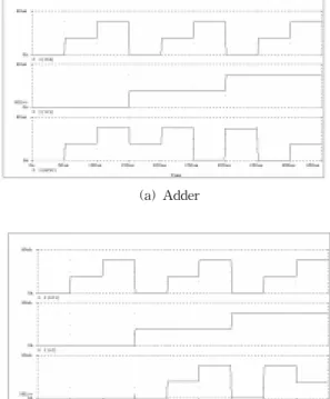
The simulation result of ternary adder and multiplier are illustrated in Fig. 4. Logical levels of the ternary input/output current are extracted as 0, 15µA and 30µA.
(a) Adder
(b) Multiplier
그림4. GF(3)상의 기본 게이트들에 대한 시뮬레이션 결과
Fig 4. Simulation result of basic gates over GF(3).
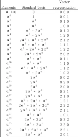
For simplicity in description, the ensuing discussion is limited to the particular finite field GF(33). The primitive irreducible polynomial is F=⍺3 +f2⍺2+f1⍺+f0⍺ = ⍺3+2⍺+1. Table 1 shows a representation of GF(33) for F = ⍺3 + 2⍺ + 1.
표1. 원시 기약 다항식 F=⍺3+2⍺+ 1에 대한 GF(33)상의 원소 표현
Table 1. Element representation of GF(33) for a primitive irreducible polynomial F=⍺3+2⍺+ 1.
It is noted that addition and multiplication of the field element ⍺0to ⍺25 result in sums and products which are, themselves, field elements. In general, modulo F(x) multiplication may be performed that each partial product generated in the simple multiplication process may be taken by modulo F(x).
When these partial products are added, the result will necessarily be a modulo F(x) result and therefore, a field element.
IV. Circuit design of highly parallel multiplier using DTOM
In this section, a new designed highly parallel multiplier using DTOM is developed to compute P=AB in GF(3m). A similar computing method was proposed to multiply the two arbitrary elements in GF(2m). For simplicity in description, the ensuing discussion is limited to the particular finite field GF(33).
In order to understand the DTOM multiplier, it is convenient to begin viewing the scheme of Fig. 5.
Fig. 5 shows a multiplier for two elements in GF(33). In Fig. 5 the multiplication is taken by modulo F(x), where F(⍺)= ⍺3 + 2⍺ + 1. The multiplier in Fig. 5 receives as input signals of two elements in GF(33) which may be represented as 3-digit input signals A and B.
The multiplicand A has digits a0, a1, a2 ; a0
being the least significant digit (LSD). The multiplier B has digits b0, b1, b2 ; b0 being the LSD.
By the previous Eq. (3), the product A⍺ may be represented as digits a0(1)
,a1(1)
, a2(1)
. DTOM 1Block shifts input signals a0(0)
,a1(0)
, a2(0)
as follows : a0(0)
to a1(1)
, a1(0)
to a2(1)
, and a2(0)
to a1(1)
and 2a0(1)
. And the three digits a0(1) ,a1(1) , a2(1) are fed into the next DTOM 2.
The DTOM Block 1 and 2 are identical; they multiply their inputs by ⍺ and produce a result modulo F(⍺), which is necessarily a 3-digit signal ; hence, they are referred to as a Digit Transition Operating Module. Also, three Ternary Multiplication computing Modules are identical; They multiply their input digits a0(m-1)
,a1(m-1)
, a2(m-1)
by bm-1, respectively and produce bm-1a0(m-1)
, bm-1a1(m-1)
, bm-1a2(m-1), respectively. Finally, Ternary Addition computing Modules are operated on their input digits, providing output signals p0, p1, p2, respectively.
The simulation result of GF(33) multiplication circuit is illustrated in Fig. 6.
Elements Standard basis
Vector representation
⍺ *=0 0 0 0 0
⍺0 1 0 0 1
⍺1 ⍺1 0 1 0
⍺2 ⍺2 1 0 0
⍺3 ⍺1 + 2⍺0 0 1 2
⍺4 ⍺2 + 2⍺1 1 2 0
⍺5 2⍺2 + ⍺1 + 2⍺0 2 1 2
⍺6 ⍺2 + ⍺1 + ⍺0 1 1 1
⍺7 ⍺2 + 2⍺1 + 2⍺0 1 2 2
⍺8 2⍺2 + 2⍺0 2 0 2
⍺9 ⍺1 + ⍺0 0 1 1
⍺10 ⍺2 + ⍺1 1 1 0
⍺11 ⍺2 + ⍺1 + 2⍺0 1 1 2
⍺12 ⍺2 + 2⍺0 1 0 2
⍺13 2⍺0 0 0 2
⍺14 2⍺1 0 2 0
⍺15 2⍺2 2 0 0
⍺16 2⍺1 + ⍺0 0 2 1
⍺17 2⍺2 + ⍺1 2 1 0
⍺18 ⍺2 + 2⍺1 + ⍺0 1 2 1
⍺19 2⍺2 + 2⍺1 + 2⍺0 2 2 2
⍺20 2⍺2 + ⍺1 + ⍺0 2 1 1
⍺21 ⍺2 + ⍺0 1 0 1
⍺22 2⍺1 + 2⍺0 0 2 2
⍺23 2⍺2 + 2⍺1 2 2 0
⍺24 2⍺2 + 2⍺1 + ⍺0 2 2 1
⍺25 2⍺2 + ⍺0 2 0 1
그림5. GF(33)상의 DTOM을 이용한 고속 병렬 승산기.
Fig. 5. A highly parallel multiplier using
DTOM over GF(33).
In Fig. 6, The arbitrary element A(a2a1a0) from first line to third line over GF(33) and of each digit value of another elements B(b2b1b0) any element from forth to sixth line are assumed. These two elements showed the multiplication result of each
digit from seventh to ninth. In 0~1.35ms, each digit of A is 000 and the multiplication result of an arbitrary B is always to be 000. Also, in 1.35ms~2.7ms, each digit of A is 001 and the multiplication result of an arbitrary B is soon shown.
α α α
+ + +
) 1 ( 2
) 1 ( 1
) 1 ( 0
i i i
=
0 1 0
1 0 1
2 0 0
α α α
) ( 2 ) 1(
) ( 0 i i i
(4) Output digits DTOM Input digits
α α α α
+− + + +
) 1 ( 1 ) 1 ( 2
) 1 ( 1
) 1 (0
mi i i i
#
=
−
−
−
−
−1 2 1 0
0 0 0
0 1 0
0 0 1
0 0 0
fm
f f f
"
#
%
#
#
#
"
"
"
α α α α
−) ( 1
) ( 2 ) ( 1 ) ( 0
mi i i i
# (5) Output digits DTOM Input digits
In 2.7ms~4.05ms, it showed the result to multiply each digit of B to mod(2). After that, each operational result is all satisfied with the operation over GF(33)
From the previous Eq. (3), the Eq. (4) shows a detailed structure of DTOM by matrix equation.
Also, the generalized structure of DTOM in GF(3m)
그림6. GF(33)상의 승산회로에 대한 시뮬레이션 결과.
Fig. 6 Simulation result of GF(33) multiplication circuit.
is shown as below Eq.(5)
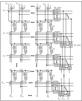
Using the Eq. (5), ternary multiplier is easy to generalize for m. Fig. 7 shows the generalized highly parallel multiplication circuit diagram over GF(3m).
b0
b1
b2
bm-1
fm-1 fm-2 f0
am-1 am-2 a0
0
0 0
P0
Pm-2
Pm-1
No. of m
2fm-1 2fm-2 2f0
f1
2f1
2 2 2 2
No. of m
그림7. GF(3m)상의 일반화된 승산회로.
Fig. 7. A generalized multiplication circuit over GF(3m).
V. Comparisons and Conclusions
5.1 Comparisons
In comparison, we compared the proposed circuit with five types of multiplier. Table 2 shows the comparisons in terms of 1-digit multiplier, 1-digit adder, MVL memory, switch, inverter, clock time and propagation delay.
Multipliers over GF(2m) need AND gates in case of 1-digit multiplication and XOR gates in case of 1-digit adder, respectively. Because existing finite field multiplicativecircuits(Law[2], Yeh[3], Wang[5], Koc[6], Parr[7]) had designed over GF(2m), they aren't enough to compare only in terms of the numerical part.
But Seong' s paper and this paper are the multiplier over GF(3m), so they mean the basic gates count in each proposed GF(3). In comparison with Seong's multiplier, the multiplier in this paper needs only the basic gate. On the other hand, Seong's multiplier needs many MV Memory, Inverter and Switch etc. From a regulation and unity point of view, we can know the proposed multiplier is more suitable to VLSI implementation.
5.2 Conclusions
In this paper, a new circuit design to perform a 표2. 승산회로 구성상의 게이트 수의 비교 표
Table 2. Comparison table of composition gates of multiplicative circuit
Terms Law[2] Yeh[3] Wang[5]
Koc[6] Parr[7] Seong[14] This paper
1-D 2-D 1-D 2-D
1-digit
Multiplier 2m2 3m 2m2 3m 2m2 m2 9m2 2m 2m2
1-digit
Adder 2m2 2m 2m2 2m 2m2 m2-1 9m2+21m- 9 2m 2m(m-1) MV
Memory - 10m+2 7m2+16 9m 2m2 - - 5m -
Switch - m - - - - - 6m -
Inverter - - - - - 2m - m -
Clock
time - 3m 3m 3m 3m - - m -
Propagation
delay 3m - - - - 2m 2m+5 - m
multiplication in GF(3m) was proposed. The architecture proposed here allows the multiplica-tive operation of two arbitrary elements of GF(33). In the previous binary logic case, the operations of addition and multiplication in a finite field are realized by AND gates and EX-OR gates, respectively. But these gates are not suitable for ternary logic circuits. So new ternary logic gates, ternary adder and ternary multiplier, are showed in this paper.
The multiplication in GF(3m) is developed by equations, newly. From these equations, we can make the multiplier circuit in GF(33), and generalized for m. This feature is to bea possibility of implementing a ternary multiplier, which could be widely used in different applications. Much future work remains. For example, hardware systems using MOS are not yet implemented in this paper and complexity is not compared with other binary and ternary multipliers. These important aspects are scheduled for further investigations.
VI. References
[1] S. B. Wicker and V. K. Bhargava, Error Correcting Coding Theory, Mc Graw-Hill, New York, 1989.
[2] B. A. Laws and C. K. Rushford, "A Cellular-Array Multiplier for GF(2m)" IEEE Trans. Computer, vol. C-20, No. 12, pp.
1573-1578, Dec. 1971.
[3] C.S. Yeh, I.S. Reed and T.K. Truong.
"Systolic multipliers for finite field GF(2m),"
IEEE Trans. Computer, vol. C-33, pp. 357-360, Apr. 1984.
[4] J.Omura and J.Massey, "Computational Method and Apparatus for Finite Field," U.S. Patent No. 4,587,627, May 1986.
[5] C.C. Wang, T.K. Truong, H.M. Shao, L.J.
Deutsch, J.K. Omura and I.S. Reed., "VLSI Architecture for Computing Multiplications and Inverses in GF(2m)," IEEE Trans. Comp., vol.
C-34, pp. 709-717, Aug. 1985.
[6] C. K. Koc. And B. Sunar, "Low-Complexity Bit Parallel Canonical and Normal Basis Multipliers for a Class of Finite Fields,"IEEE Trans. Comp., Vol. 47, No. 3, pp. 353-356. Mar.
1998
[7] C. Paar, P. Felishmann, and P. Roelse,
"Efficient Multiplier Architectures for Galois Fields FG((24)n)", IEEE Trans. Comp., Vol.
C-47, No. 2, pp. 162-170. Feb. 1998.
[8] J.C. Muzio, "Introduction Multiple-Valued Logic," IEEE Trans. Comp., vol. 35, pp.97-98.
Feb. 1986.
[9] J.T.Butler, "Multiple-Valued Logic : guest editor's introduction and bibliography" IEEE Comp. Mag., vol. 21, pp.13-15. Apr. 1988.
[10] K. C. Smith, "The Prospect for Multivalued Logic : A Technology and Applications View,"
IEEE Trans. Comp., Vol. C-30, No. 9, pp.
619-634, Sept. 1981.
[11] N. Kamiura, Y. Hata and K. Yamato, "Design of a Multiple-Valued Cellular Array," IEICE Trans. Electron., vol. E76-C, No. 3 pp. 412-418, March . 1993.
[12] T.Hanyu, S.Kazama, M.Kameyama, "Design and implementationof a Low-Power Multiple-Valued Current Mode Integrated Circuit with Current-Source Control,"
IEICETrans. Electron vol. E80-C, No. 7 pp. 941-947, July. 1997.
[13] Y. Hata, N. Kamiura, and K. Yamato,"Design of Multiple-Valued Programming Logic Array with Unary Function Generators," IEICE Trans.
Inf. & Syst., vol. E82-D, No. 5 pp. 933-939, May. 1999.
[14] H. K. Seoung, J. S. Choi, B. S. Shin, H. S.
Kim, "Implementation of Multiple-Valued Multiplier on GF(3m) Using Current Mode CMOS," IEEE Proc. 30th ISMVL, pp. 221-226, May 2000.
[15] A. Gill, Linear Sequential Circuits, McGraw-Hill Book Co., Newyork. 1966.
[16] S. Lin, Error Control Coding, Prentice-Hall, Inc. New Jersey, 1983.
[17] P. Sweeney, Error Correcting Coding An
Introduction, Prentice-Hall, Inc. New Jersey, 1991.
저 자 소 개
나 기 수 (Gi-Soo Na) 정회원 1997년 2월 : 건양대학교 컴퓨터공학과 (공학사)
1999년 2월 : 인하대학교 대학원 전자공학과 (공학석사)
1999년 3월 - 현재 : 인하대학교 대학원 전자공학과 박사과정 2001년 2월 ∼ 2002년 10월 : (주)크리텔 회로 설계 연구원
<주관심 분야> 디지털 로직, 오류정정부호 설계, VHDL, Soc 설계, VLSI 회로구현
변 기 영 (Gi-Young Byun) 정회원 1994년 2월 : 인하대학교 전자공학과 (공학사)
1998년 8월 : 인하대학교 대학원 전자공학과 (공학석사)
2003년 2월 : 인하대학교 대학원 전자공학과 (공학박사)
1994년 1월 ∼ 1996년 8월 : (주)LG전자 VCR사업부 회로설계연구원 2003년 3월 ∼ 현재 : 가톨릭대학교 정보통신 전자공학부 강의전담교수.
현재 IEEK, KICS 정회원, IEICE 해외회원
<주관심분야> 정보 및 부호이론,논리시스템설계, 컴퓨터 구조, 유한체 이론의 응용 및 VLSI 회로구현 등
김 흥 수 (Heung-Soo Kim) 정회원 제 7 권 1호 논문 03-01-05 참조 인하대학교 전자공학과 교수