1. 서 론
무분극(nonpolar) GaN 반도체는 분극이 없는 특성 으로 인하여 고효율 광전자소자로의 적용에 많은 관심 을 끌고 있다. 분극(polarization) 전기장은 공간적으 로 분리된 전자와 정공의 파동함수를 야기 시킴으로써 양자우물에서의 발광 재결합을 감소시키게 된다. 많은 연구자들은 무분극 a-plane (11-20) GaN와 반분극 (semipolar) m-plane (1-100) GaN 반도체가 이러한 분극 전기장이 없는 특성을 보임을 제시하였으며, 최근 에는 무분극 a-plane (11-20) GaN와 반분극 m-plane
a. Corresponding author; [email protected] Copyright ©2017 KIEEME. All rights reserved.
This is an Open-Access article distributed under the terms of the Creative Commons Attribution Non-Commercial License (http://creativecommons.org/licenses/by-nc/3.0) which permits unrestricted non-commercial use, distribution, and reproduction in any medium, provided the original work is properly cited.
(1-100) GaN 기반 LED의 발광효율을 증대시키기 위 한 연구를 많이 진행하고 있다 [1-10].
특히 편극 특성의 c-plane GaN LED 뿐만 아니라 무분극 a-plane GaN LED의 경우, 현재까지도 질화갈 륨계 발광다이오드 소자 동작 시 질화갈륨층으로의 원 활한 전류 퍼짐 즉 확산전류는 여전히 이슈가 되고 있 다. 이는 수평형 방식으로 빛을 내는 소자에서는 p-type 질화갈륨층의 정공(hole) 농도가 낮고 저항이 높아짐으 로 인해 전류 퍼짐이 좋지 않은 것이 주 원인으로 보고 되고 있다. ITO (indium tin oxide)와 같은 투명 확산 층에도 불구하고 활성 층으로 주입 되어 광자로 변환된 전자의 일부가 두꺼운 접착 패드 금속(bonding pad metal)에 갇히게 되어 상당한 양의 빛이 흡수되거나 갇혀 휘도감소의 원인이 된다. 이와 같이 패드 금속 (pad metal)에 흡수되는 현상을 개선하기 위하여 제안 된 기술이 전류 제한 층(current blocking layer, CBL)
무분극 a-plane 질화물계 발광다이오드에서 SiO
2전류 제한 층을 통한 발광 효율 증가
황성주, 곽준섭
a
순천대학교 인쇄전자공학과
Improvement of the Light Emission Efficiency on Nonpolar a-plane GaN LEDs with SiO 2 Current Blocking Layer
Seong Joo Hwang and Joon Seop Kwak a
Department of Printed Electronics Engineering, Sunchon National University, Sunchon 57922, Korea (Received December 23, 2016; Revised January 10, 2017; Accepted January 26, 2017)
Abstract: In this study, we investigate the SiO 2
current blocking layer (CBL) to improve light output power efficiency in nonpolar a-plane (11-20) GaN LEDs on a r-plane sapphire substrate. The SiO2
CBL was produced under the p-pad layer using plasma enhanced chemical vapor deposition (PECVD). The results show that nonpolar GaN LED light output power with the SiO2
CBL is considerably enhanced compared without the SiO2
CBL. This can be attributed to reduced light absorption at the p-pad due to current blocking to the active layer by the SiO2
CBL.
Keywords: Nonplar LED, a-plane, GaN, Current blocking layer
ISSN 1226-7945(Print), 2288-3258(Online)
보고되었다. 이후, p-GaN 구조에 대한 plasma selective treatment [12], current-blocking hole [13], 그리고 selective activated CBL [14] 등의 기술 들이 보고되었다. 하지만 위의 많은 연구자들은 c-plane GaN를 기반으로 한 LED에 기술을 적용하였으며, 무 분극 GaN 기반에는 아직까지 적용을 하지 않고 있는 실정이다.
이에 본 연구는 PECVD를 이용하여 무분극 a-plane p-GaN 상부에 SiO
2
CBL을 형성하고, SiO2
CBL로 인 하여 p-형 접착 패드 금속과 n-metal 간 경로를 중심 으로 활성층에 주입되는 전류를 차단하여, 패드 금속에 광이 흡수되는 것을 줄이고 전류 퍼짐을 향상시킴으로 써 무분극 a-plane GaN LED의 광추출 효율을 향상 시키는 연구를 진행하였다.2. 실험 방법
먼저 무분극 a-plane GaN LED를 제작하기 위하여 metal organic chemical vapor deposition (MOCVD) 를 이용하여 r-plane sapphire에 4 um 두께의 a- plane GaN를 성장하였다. 이후 2 um 두께의 Si이 도 핑된 n-type a-plane GaN를 성장하였으며, 무분극 a-plane InGaN 단일 양자우물(quantum well), 150 nm 두께의 Mg이 도핑된 p-type a-plane GaN를 성 장하였다. 상기에 제작한 무분극 a-plane GaN LED 구조를 inductive coupled plasma (ICP)를 이용하여 MESA 건식 식각을 진행하였다. 이때 positive photo resist (PR)을 식각마스크로 이용하였으며, n-type 무 분극 a-plane GaN를 노출시키고자 1 um 이상 건식 식각을 진행하였다. 이후 CBL을 형성하고자 PECVD를 이용하여 wafer 전면에 SiO
2
를 150 nm 두께로 형성 하였다. 이후 positive PR을 이용하여 p-전극보다 5 um 이상 큰 패턴을 형성하고 buffered oxide etchant (BOE)를 이용하여 습식식각을 진행하여 p-패 드 보다 넓은 SiO2
CBL층을 형성하였다. 그런 다음, 전자선 증착기(elctron-beam evaporator)를 이용하(current-voltage) 특성과 전류-radiant intensity 특 성 및 인가전류에 따른 electro-luminescence (EL) 특성은 universal LED tester로 측정하였다.
3. 결과 및 고찰
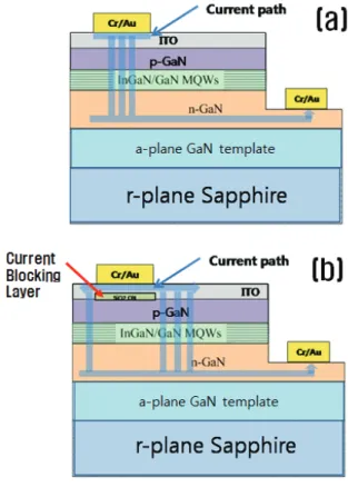
그림 1(a)는 CBL이 없는 일반적인 무분극 a-plane GaN LED의 전류 주입시 전류의 흐름에 대한 간략한 구조이며, 그림 1(b)는 CBL이 삽입된 a-plane GaN LED의 전류 주입 시 전류의 흐름에 대한 간략한 구조 에 대하여 묘사하였다. 일반적인 a-plane GaN LED의
Fig. 1. A schematic diagram of non-polar a-plane GaN LEDs
(a) without the CBL and (b) with the CBL.
경우 수평형 방식으로 빛을 내는 소자에서는 p-형질화 갈륨층의 정공 농도가 낮고 저항이 높아짐으로 인해 전류 퍼짐이 좋지 않은 것이 주원인으로 보고되고 있 다 [15,16]. ITO와 같은 투명 확산 층에도 불구하고 활성 층으로 주입되어 광자로 변환된 전자의 일부가 두꺼운 접착 패드 금속에 갇히게 되어 상당한 양의 빛 이 흡수되거나 갇혀 휘도감소의 원인이 된다. 이런 문 제를 해결하기 위하여 그림 1(b)와 같이 CBL층을 이용 하여 전류의 퍼짐을 좋게 하기 위하여 소자를 제작하 였다.
그림 2(a)는 SiO
2
CBL이 삽입된 a-plane GaN LED 의 사진이다. LED 소자의 크기는 1,000×1,000 um2
이다. 그림 2(b)는 a-plane GaN LED의 p-전극 부분 을 확대한 현미경 사진이다. 그림 2(b)에서 보는 바와 같이 p-전극 하부에 SiO2
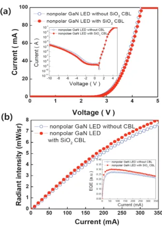
CBL이 존재 하는 것을 확인 할 수 있다.그림 3(a)는 CBL이 없는 무분극 a-plane GaN LED 와 SiO
2
CBL이 삽입된 무분극 a-plane GaN LED의 전기적 특성을 보여주는 그래프이다. 그림 3(a)에서 CBL이 없는 무분극 a-plane GaN LED의 경우 20 mA에서 3.47 V, SiO2
CBL이 삽입된 무분극 a-plane GaN LED의 경우 3.56 V로 전기적 특성에서 SiO2
CBL이 삽입된 무분극 a-plane GaN LED의 경우 0.09 V 증가한 것을 알 수 있다. 이는 SiO
2
CBL 삽입 으로 p-GaN에 접촉되는 ITO의 면적이 줄어듦에 따른 접촉저항의 증가에 기인한다고 사료된다. 그림 3(a)에 삽입된 그림은 역전류(reverse current) 특성을 보여주 는 그림으로, -5 V에서 측정된 역 전류는 SiO2
CBL의 유무에 관계없이 1 μA 이하로 측정되어 양호한 역 누 설전류(reverse leakage current) 특성을 나타내었다.그림 3(b)는 CBL이 없는 무분극 a-plane GaN LED와
SiO
2
CBL이 삽입된 무분극 a-plane GaN LED의 광 학적 특성에 관한 그래프이다. 250 mA에서 CBL이 없 는 무분극 a-plane GaN LED와 SiO2
CBL이 삽입된 무분극 a-plane GaN LED의 radiant intensity는 각 각 6.04 mW/sr과 6.54 mW/sr으로 CBL이 없는 무 분극 a-plane GaN LED 보다 SiO2
CBL이 삽입된 무 분극 a-plane GaN LED가 8.27% 증가하였다. 그림 3(b)에 삽입된 그림은 CBL이 없는 무분극 a-plane GaN LED와 SiO2
CBL이 삽입된 무분극 a-plane GaN LED의 인가 전류 변화에 따른 외부양자효율 (external quamtum efficiency, EQE)특성을 보여준 다. CBL이 없는 무분극 a-plane GaN LED와 SiO2
CBL이 삽입된 무분극 a-plane GaN LED의 EQE는 50 mA에서 최고값을 가지는 것을 확인할 수 있으며, 전
Fig. 3. (a) Current-voltage characteristics for nonpolar a-plane GaN LED with/without SiO 2 CBL, and the inserted figure shows the reverse leakage characteristics for both the LEDs and (b) variation of radiant intensity as a function of applied current for nonpolar a-plane GaN LED with/without SiO 2
CBL, and the inserted figure shows external quantum efficiency for both the LEDs.
Fig. 2. Optical microscope image of (a) nonpolar a-plane GaN LED and (b) enlarged image of the circle area in Fig.
2(a).
반적으로 EQE는 SiO
2
CBL이 삽입된 무분극 a-plane GaN LED가 CBL이 없는 무분극 a-plane GaN LED 에 비하여 높은 것을 알 수 있었다.그림 4(a)와 (b)는 각각 CBL이 없는 무분극 a-plane GaN LED와 SiO
2
CBL이 삽입된 무분극 a-plane GaN LED에 대하여 전류 증가에 따른 EL 변화를 보 여주는 그림이다. 두 LED 모두 전류가 20 mA에서 350 mA로 증가할수록 EL spectrum의 강도가 지속적으로 증가하여 전류 주입 증가에 따른 EL특성의 향상 을 알 수 있었고, 모든 전류 값에서 EL 특성은 SiO
2
CBL이 삽입된 무분극 a-plane GaN LED가 CBL이 없 는 무분극 a-plane GaN LED에 비하여 높게 나타나 서 발광효율이 높게 나타났으며, 이는 그림 3(b)의 radiant intensity와 EQE와 동일한 경향을 보이는 결 과이다. 그림 4(c)는 입력 전류가 20 mA에서 350 mA 로 증가됨에 따른 EL의 peak wavelength의 변화를 보여준다. CBL이 없는 무분극 a-plane GaN LED와 SiO
2
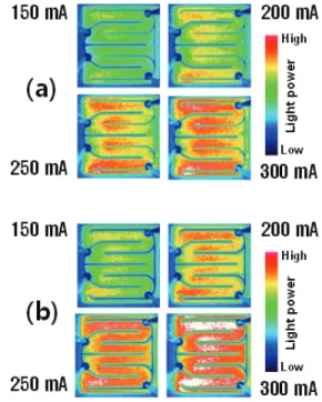
CBL이 삽입된 무분극 a-plane GaN LED모두 peak wavelength의 변화는 2 nm 이내로 매우 작은 값을 나타내었다. 이는 polar GaN LED의 경우 10 nm 이상의 peak wavelength변화를 나타내는 결과와 극명한 차이를 보이는 결과로, nonpolar GaN LED의 고유한 특성을 잘 보여주는 결과이다.그림 5(a)와 (b)는 150~300 mA 전류 인가 시 각각 CBL이 없는 무분극 a-plane GaN LED와 SiO
2
CBL 이 삽입된 무분극 a-plane GaN LED의 발광 분포를 나타낸 그래프이다. 상기 그림 5에서의 광학적 특성에 서 보는 바와 같이 CBL이 없는 무분극 a-plane GaN LED에 비하여 SiO2
CBL이 삽입된 무분극 a-plane GaN LED의 경우 전류 퍼짐(current spreading)의(b)
(c)
Fig. 4. Variation of EL spectrum as a function of applied current for (a) nonpolar GaN LED without CBL and (b) nonpolar GaN LED with SiO 2 CBL. (c) Variation of peak wavelength as a function of applied current for both the LEDs.
Fig. 5. Emission distribution of the nonpolar GaN LED
without CBL (a) and the nonpolar GaN LED with SiO 2 CBL
(b) at applied current of 150, 200, 250, and 300 mA.
특성이 150~300 mA 전류 인가 모두에서 우수한 것을 확인할 수 있다. 이는 SiO
2
CBL로 인하여 p-형 접착 패드 금속과 n-전극 간 경로를 중심으로 활성층에 주 입되는 전류를 차단하여 다른 경로로 전류를 보냄으로 써, 전류 퍼짐을 향상시키게 되었고 활성층에서 나온 광이 패드 금속에 흡수되는 것을 줄이게 되어, 광 출 력이 상당 부분 개선되는 것을 확인할 수 있었다. 이 는 그림 3과 4의 결과와 같이 SiO2
CBL이 무분극 a-plane GaN LED의 radiant intensity, EQE 및 EL 특성을 향상시키는 결과와 일치하며, 무분극 a-plane GaN LED의 광특성을 향상시키는데 있어서 SiO2
CBL 이 유효한 기능을 한다는 것을 보여준다.4. 결 론
본 논문에서는 무분극 a-plane GaN 발광다이오드 의 광 추출 효율을 상승시키기 위하여, SiO
2
를 CBL층 으로 형성하여 광 추출 효율 증가 효과를 연구하였다.SiO
2
CBL을 p-GaN와 ITO 층 사이에 형성함으로서, 일반적인 무분극 a-plane GaN LED 보다 CBL 층이 형성된 무분극 a-plane GaN LED가 250 mA에서 8.27% 향상된 발광 효율을 나타내었다.이는 SiO
2
CBL로 인하여 p-형 접착 패드 금속과 n-metal 간 경로를 중심으로 활성층에 주입되는 전류 를 차단하여, 패드 금속에 광이 흡수되는 것을 줄이고 전류 퍼짐을 향상시킴으로써, 발광 효율이 상당 부분 개선되는 것으로서, 이로부터 SiO2
CBL이 무분극 a-plane GaN LED의 광특성을 향상시키는데 있어서 유효한 기능을 한다는 것을 알 수 있었다.감사의 글
본 논문은 2016년 순천대학교 학술연구비로 연구되었음.
REFERENCES