Received 26 June 2016, Revised 4 July 2016 Accepted 8 July 2016
Corresponding Author: Teresa Oh(Cheongju Unversity) Email: [email protected]
Ⓒ Industrial Promotion Institue. All rights reserved. This is an open-access article distributed under the terms of the Creative Commons Attribution Non-Commercial License (http://creative commons.org/licenses/by-nc/3.0), which permits unrestricted non-commercial use, distribution, and reproduction in any medium, provided the original work is properly cited.
ISSN: 2466-1139
ZTO 박막의 열처리온도에 따른 결정성과 전기적인 특성 연구
조윤정
*
, 채홍주**
, 오데레사***
청주대학교 반도체공학과
Study on Electrical Properties and Structures of ZTO Thin Films Depending on the Annealing Temperature
Yun Jung Jo * , Hong Ju Chae ** , and Teresa Oh ***
Dept. of Semiconductor, Cheongju University
요 약 ZTO
의 결정성의 변화에 따른 전기적인 특성을 조사하기 위해서 진공 중에서 열처리를 하여 , 전류전압 특성 을 조사하였다 . ZTO 박막은 진공 중에서 열처리를 하면 계면에서 접합효과에 의해 많은 결함들이 생기고 이온화에 의해 공핍층이 생성된다 . 결함과 공핍층의 형성은 열처리 온도에 따라서 달라지며 , 결정성 , 결합에너지는 물론 결과 적으로 전하량의 변화에 의해 전기적인 특성이 변화하는 것을 알 수 있었다 . ZTO 박막은 열처리하면서 결정성이 높 아졌으며 , 150 도 열처리한 ZTO 박막에서 전기적으로 많은 전류가 형성되는 것을 확인하였다 .
주제어 : ZTO, XRD, XPS,
결합에너지 , 쇼키 접합
Abstract ZTO films were annealed in a vaccum atmosphere conditions to research the temperature dependency of current-voltage characteristics. The ZTO film annealed in a vacuum became an amorphous structure but films annealed in an atmosphere condition had a crystal structure. The defects or depletion layer were formed by the electron-hole combination after annealing processes, and the electrical properties were changed depending on the crystal structure, binding energy and the variation of carriers. ZTO became more crystal-structural with increasing the annealing temperature, and the current increased at ZTO film annealed at 150 ℃ with Schottky contact.
Key Words : ZTO, XRD, XPS, Binding energy, Schottky contact
1. 서론
Zinc tin oxide(ZTO)는 넓은 밴드 갭을 특징으로 하는 산화물 반도체 중 하나이다. ZTO를 비롯한 산화물반도 체의 높은 결정화 온도는 반도체계면효과에 의한 공핍층
의 형성과 연관이 있다. ZTO는 화학적으로 안정하여 쉽 게 산화하거나 부식되지 않으며, 물리적인 특성도 우수 하여 흠집에 대해 강한 내성을 가지고 있다[1-3]. 1907년 Bädeker에 의해 CdO박막이 처음으로 만들어진 이래로 ZnO계, SnO2계,In2O3계 혼합물이 투명전도체 박막으로
알려졌으며, 이러한 산화 물들의 첨가는 광 투과도 와 전 기 전도성을 향상시켰다. TCO의 대표적인 물질 중 하나 인 Zinc Oxid e(ZnO) 기반 TFT는 a-si에 비해 높은 Mobi lity를 가지고 고속 회로 구동이 가능하며 저온 진 공공정에서의 제작이 가능한 특징이 있다. 또한 상대적 으로 넓은 밴드 갭(Wide band gap, 3.3eV)을 갖고 있 으 며 높은 Binding energy를 갖는다. 이러한 장점때문에 AMOLED 와flexible 디스플레이와 같은 차세대 디스플 레이 소자로의 활용성이 높다[4-7]. 기존의 Si반도체는 Valence band의 전자가 Conduction band로 여기 되는 현상으로 인해 대부분의 빛 에너지가 흡수되어 투과도가 떨어지는 문제가 있는 반면에 산화물 반도체는 3eV이상 의 넓은 밴드 갭을 가지기 때문에 가시광선의 흡수가 거 의 일어나지 않아 투명 소자 제작이 가능하다.[8-13]
본 논문에서는 ITO 유기 기판위에 ZTO 박막을 증착 하여, 열처리온도에 따른 결정성, 산소관련 결합에너지의 변화로부터 전기적인 특성이 어떻게 변화하는가를 관찰 하였다.
2. 실험방법
ZTO박막은 ITO 유리기판 위에 ZTO 타겟을 사용하 고 아르곤과 산소 혼합가스(Ar:O2=5 sccm:17 sccm)를 주입하여 70 W 파워의 플라즈마를 형성하였으며, RF magnetron sputtering장비를 이용하여 10분동안 증착하 였다. 증착이 된 ZTO박막은 진공에서 각각 RT, 100℃∼
250℃에서 열처리를 10분동안 실시하였으며, 각가의 박 막들의 분석은 X-ray diffraction (XRD), X-ray photoelectron spectrascopy (XPS)를 이용하여 결정성과 화학적인 특성을 조사하고 전기적인 특성과의 상관성을 조사하였다. 전기적인 특성을 조사하기 위해서 Al 전극 을 이용하여 Al/ZTO/ITO 유리의 구조를 이용하여, I-V 특성을 측정하여 반도체 계면특성에 대하여 조사하고 열 처리 온도에 따른 특성을 조사하였다.
3. 결과 및 데이터 분석
ZTO 박막은 ZnO:SnO2=1:1의 비율로 파우터 형태를 소결시켜서 만들어지는 타겟이다. 따라서 ZnO와 SnO2
물질의 특성을 모두 갖고 있으면서 ZTO 박막의 물리적 특성와 전기적인 특성이 어떤 영향을 받는지를 조사하기 위해서 XRD 분석, XPS과 I-V 특성을 측정하였다.
29.6 30.0 30.4 30.8 31.2
30.4
ZTO 200
oC
150
oC
100
oC RT
2 theta
In tens ity ( a rb.u nits)
(a) XRD patterns near 30.4
o(degree)
34.2 34.5 34.8 35.1 35.4 35.7 36.0 36.3 35.3
ZTO 200
oC
150
oC
100
oC RT
2 theta
Intensity (arb.units)
(b) XRD patterns near 35.3
o(degree)
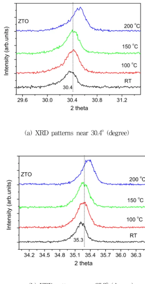
[Fig. 1] XRD patterns of ZTO thin films after annealing in a vacuum condition
Fig. 1은 진공 중에서 열처리한 ZTO박막의 XRD 패턴 을 보여준다. 증착한 ZTO 박막은 결정질특성을 나타내 고, 200도에서도 결정질특성을 나타냈다. 30.4o (degree) 와 35.3o (degree)에서 픽이 나타나며 결정성이 보이는데 열처리온도가 증가할수록 높은 쪽으로 이동하는 것을 알 수 있다.
이러한 특성은 산화물반도체에서 일어나는 일반적인 특성과 다른 특이한 결과를 나타낸다. AZO, ZnO 혹은 GTO와 같은 n-타입의 산화물반도체는 열처리 온도가 증가할수록 결정성이 높아지면서 33.5o (degree)에서
XRD 패턴이 나타난다. 그리고 비정질 IGZO 박막의 경우 에는 열처리를 하면 33.5o (degree)에서나는 XRD 픽이 사라진다[4]. 그런데 ZTO인 경우 33.5o (degree)가 아닌 30.4o (degree)와 35.3o (degree)에서 XRD 패턴이 나타난 것을 알 수 있다. 이는 p-타입의 SnO2의 영향에 의해서 결정면이 달라지면서 나타나는 효과임을 알 수 있다.
526 527 528 529 530 531 532 533 534 535 536
ZTO
250
oC 200
oC
150
oC RT
O 1s intens ity ( ar b.units)
Binding energy (eV)
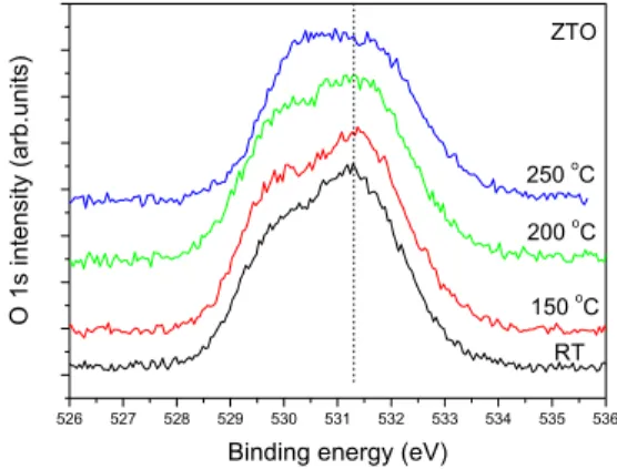
[Fig. 2] O 1s spectra of ZTO thin films after annealing in a vacuum condition analyzed by XPS patterns
-30 -20 -10 0 10 20 30
0.0 5.0x10
-121.0x10
-111.5x10
-11RT 150
oC
Voltage (V) RT
100
oC 150
oC 200
oC 250
oC
Ca pa cit a nce (F)
[Fig. 3] Capacitance of ZTO thin films with various annealing temperature
그림 2는 산소공공과 연관이 있는 ZTO 박막을 구성 하는 원자들 중 산소와 관련된 결합에너지를 알 수 있는 XPS 스펙트라이다. 열처리 온도가 증가할수록 결합에너 지는 낮은 방향으로 이동하고 있으며, 산소와 관련된 원 자들과의 결합력이 작아지고 있음을 알 수 있다. 일반적
인 산화물반도체는 온도가 증가하면서 결정성이 높아지 고 O 1s 값도 높아지는 경향이 있는데[4] ZTO의 경우에 는 O 1s 값이 크게 변하지는 않으면서 531 eV에서의 O 1s 결합의 모양에서 조금씩 차이가 있는 것을 보여준다.
이러한 현상 또한 p-타입의 SnO2의 영향에 의한 것임을 알 수 있다.
그림 3은 열처리 온도에 따른 ZTO의 케리어 생성에 의한 전하량을 알 수 있는 커패시턴스를 나타내고 있다.
증착한 경우에 전하량이 증가하였으며, 열처리함에 따라 전하량 감소에 의하여 커패시턴스 값이 매우 급격히 감 소하였다. p-타입의 SnO2의 영향에 의해서 열처리 후 급격히 전하의 양이 감소하는 것을 알 수 있다.
-30 -20 -10 0 10 20 30
8.0x10
-141.0x10
-131.2x10
-131.4x10
-131.6x10
-13250
oC 100
oC 200
oC 150
oC
Voltage (V)
Capacitance (F )
[Fig. 4] Capacitance of ZTO thin films after annealing in a vacuum condition
-5 -4 -3 -2 -1 0 1 2 3 4 5
-5.0x10
-10-4.0x10
-10-3.0x10
-10-2.0x10
-10-1.0x10
-100.0 1.0x10
-102.0x10
-103.0x10
-104.0x10
-105.0x10
-10RT 200
oC 250
oC
100
oC 150
oC
Current (A)
Voltage (V)
RT 100 oC 150 oC 200 oC 250 oC
[Fig. 5] Current-voltage characteristics of ZTO thin films
그림 4는 열처리된 ZTO 박막의 커패시턴스를 나타내 며, 150도 온도에서 열처리한 박막이 가장 큰 커패시턴스 값을 나타낸다. 열처리한 샘플만을 비교해 보았을 때 열
처리 온도가 증가하면서 양의 전하량에 해당하는 산소공 공 (Vo2+)이 생성되면서 전하양이 많아지기 때문에 온도 가 높을수록 커패시터가 증가하였다. 그런데 250도에서 는 다시 감소하는데 이는 온도가 너무 증가하게 되면 진 공 중에서 열처리하는 과정에서 산소공공이 생성되다가 높은 온도에 의해서 박막의 두께가 극도로 얇아지면서 산소공공이 깨어지고 다시 산소공공의 양이 줄어들기 때 문인 것으로 볼 수 있다.
그림 5는 ZTO 박막의 열처리 온도에 따른 전기적인 특성을 나타낸다. 증착한 박막과 150도 열처리한 박막에 서 전류가 가장 많이 흐르고 있다.
-30 -20 -10 0 10 20 30
-1.5x10
-5-1.0x10
-5-5.0x10
-60.0 5.0x10
-61.0x10
-5RT 150
oC
Current (A)
Voltage (V)
RT 100 oC 150 oC 200 oC 250 oC
[Fig. 6] Current-voltage characteristics of ZTO thin films
그림 6은 증착한 박막과 150도 열처리한 박막에서 흐 르는 전류량을 비교하고 있다. 증착한 경우 ZTO 박막은 오믹접합을 나타내지만 150도 열처리한 박막은 쇼키 접 합을 나타내고 있다.그림 2에서 O 1s 픽이 150도에서 가 장 높게 나타났으며, 그림 4와 5에서 보듯이 열처리한 뒤 전하량의 증가에 의한 전류증가 현상을 보여주는 박막은 150도 공정에서 이루어진 ZTO박막이었다. ZTO 박막은 열처리 후 계면에서 전자홀 쌍의 재결합에 의하여 공핍 층이 증가하며, 공핍층의 증가에 의해서 쇼키접합이 만 들어지는데 쇼키접합에 의하여 계면의 특성이 달라지며, 달라진 계면특성은 온도에 따라서 트랩이 발생한다. 트 랩은 이온화 되지 못한 결함들로서 전하의 산란 현상을 유발하여 전류의 흐름을 방해하기도 한다. 따라서 150도 열처리를 한 경우 ZTO 박막의 계면은 결합이 없는 공핍 층을 형성합으로써 이상적인 쇼키접합을 형성하게 되고
반도체 소자에서 효율을 증배시킬 수 있는 특성을 갖게 되는 것을 알 수 있다.
4. 결론
ZTO 박막은 결정질특성일 때 좋은 특성을 갖는 것으 로 알려져 있으며, 열처리 온도에 따라서 결정질 특성은 달라졌으며, 진공 중에서 열처리후 30.4o (degree)와 35o (degree)에서 나타나는 결정성 픽은 열처리 하면서 높은 쪽으로 점점 이동하였다. XRD 픽의 위치가 이동하는 것 은 결정질의 정도가 다르기 때문이며, 150도에서 열처리 한 경우의 O 1s 스펙트라에 의한 결합에너지는 가장 높 았으며, 전하량이 증가하여 전류도 증가하는 것을 확인 하였다. 따라서 ZTO 박막은 150도 진공열처리 공정에서 전기적인 특성이 우수하게 나타나는 것을 확인하였다.
References
[1] Sung Hoon Oh, Sae Won Kang, Gun Hwan Lee, Woo Seok Jung, Pung Keun Song,“Effect of Annealing on the Electrical Property and Water Permeability of ZTO/GZO Double-layered TCO Films deposited by DC, RF Magnetron Co-sputtering", The Korean Institute of Surface Engineering, Vol. 45, pp 34-45, 2012.
[2] H. M. Kim and J. J. kim, “Heat Treatment Effects on the Electrical Properties of In2O3-ZnO Films Prepared by RF-Magnetron Sputtering Method,” J.
Korean Vacuum Society, Vol. 14, pp. 238-244, 2005.
[3] Teresa Oh “Analysis of Electrical Characteristics of Oxide Semiconductor of ZnO, SnO2 and ZTO”
Korean Journal of Materials Research, Vol. 25 pp.
347-349, 2016.
[4] Young Deuk Ann, Jae Ho Yeon and Teresa Oh,
“Comparison between the Electrical Properties and Structures after Atmosphere Annealing and Vaccum Annealing of IGZO Thin Films,” Industry Promotion Research, Vol. 1, pp. 1-6, 2016.
[5] Meng Yu and Jungyol Jo, “Sputtering Growth of
ZnO Thin-Film Transistor Using Zn Target”, The Journal of the Korean Institute of Electrical and Electronic Material Engineers, September Vol. 13, pp. 35-38, 2014.
[6] Kyoungjin Kim and Joong-Youn Park, “Effects of Forced Self Driving Function in Silicon Wafer Polishing Head on the Planarization of Polished Wafer Surfaces”, The Journal of the Korean Institute of Electrical and Electronic Material Engineers, March 2014. Vol. 13, No. 1, pp 13-17.
[7] Dukyean Yoo, Hyoungju Kim, Junyeong Kim and Jungyol Jo, “Current Variation in ZnO Thin-Film Transistor under Different Annealing Conditions”, Journal of the Semiconductor & Display Technology, Vol. 13, pp. 63-66, 2014.
[8] Chu, M.C., Meena, J.S., Liu, P.T., Shieh, H.D., You, H.C., Tu, Y.W., Chang, F.C., and Ko, F.H., “Oxygen Plasma Functioning of Charge Carrier Density in Zinc Oxide Thin-Film Transistors,” Applied Physics Express, Vol. 6, 076501, 2013.
[9] Young Ho So, Jung Ho Song, Dong Myung Seo and Teresa Oh, “A Study on the Chemical Properties of AZO with Crystral Structure and IGZO of Amorphous Structure due to the Annealing Temperature,” Industry Promotion Research, Vol. 1, pp. 1-6, 2016.
[10] D. H. Hwang, H. H. Ahn, K. N. Hui, K. S. Hui, and Y. G. Son, “Effect of Oxygen Partial Pressure Contents on the Properties of Al-doped ZnO Thin Films Prepared by Radio Frequency Sputtering,” J.
Ceram. Proc. Res., Vol. 12, pp. 150-154, 2011.
[11] Chu, M. C., Meena, J.S., Liu, P.T., Shieh, H.D., You, H.C., Tu, Y.W., Chang, F.C., and Ko, F.H.,
“Oxygen Plasma Functioning of Charge Carrier Density in Zinc Oxide Thin-Film Transistors,”
Applied Physics Express, Vol. 6, 076501, 2013.
[12] B. K. Lee and K. M. Lee, “Structural and Electrical Characteristics of IZO Thin Films Deposited on Flexible Substrate”, The Journal of the Korean Institute of Electrical and Electronic Material Engineers, Vol. 10, pp. 39-44, 2011.
[13] D. H. Hwang, H. H. Ahn, K. N. Hui, K. S. Hui, and Y. G. Son, “Effect of Oxygen Partial Pressure Contents on the Properties of Al-doped ZnO Thin Films Prepared by Radio Frequency sputtering,” J.
Ceram. Proc. Res., Vol. 12, pp. 150-154, 2011.
조 윤 정(Jo, Yun Jung)
․청주대학교 반도체공학과 재학
․관심분야 : 반도체소자
․E-Mail : [email protected]
채 홍 주(Chae, Hong Ju)
․청주대학교 반도체공학과 재학
․관심분야: 반도체공정
․E-Mail : [email protected]
오 데레사(Oh, Teresa)