공융 갈륨-인듐 액체금속 전극 기반 전기이중층 커패시터
김지혜⋅구형준†
서울과학기술대학교 화공생명공학과
An Electric Double-Layer Capacitor Based on Eutectic Gallium-Indium Liquid Metal Electrodes
JI-HYE KIM, HYUNG-JUN KOO
†Department of Chemical and Biomolecular Engineering, Seoul National University of Science and Technology, 232 Gongneung-ro, Nowon-gu, Seoul 01811, Korea
†
Corresponding author :
[email protected]Received
16 November, 2018Revised
6 December, 2018Accepted
30 December, 2018Abstract >> Gallium-based liquid metal, e.g., eutectic gallium-indium (EGaIn), is highly attractive as an electrode material for flexible and stretchable devices. On the liquid metal, oxide layer is spontaneously formed, which has a wide band-gap, and therefore is electrically insulating. In this paper, we fabricate a capacitor based on eutectic gallium-indium (EGaIn) liquid metal and investigate its cyclic voltammetry (CV) behavior. The EGaIn capacitor is composed of two EGaIn elec- trodes and electrolyte. CV curves reveal that the EGaIn capacitor shows the be- havior of electric double-layer capacitors (EDLC), where the oxide layers on the EGaIn electrodes serves as the dielectric layer of EDLC. The oxide thicker than the spontaneously-formed native oxide decreases the capacitance of the EGaIn capacitor, due to increased voltage loss across the oxide layer. The EGaIn capaci- tor without oxide layer exhibits unstable CV curves during the repeated cycles, where self-repair characteristic of the oxide was observed. Finally, the electrolyte concentration is optimized by comparing the CV curves at various electrolyte concentrations.
Key words : Liquid metal(액체금속), Eutectic gallium-indium(갈륨-인듐 공융합금), Electric double-layer capacitor(전기 이중층 커패시터), Electrochemistry(전기화학), Gallium oxide(갈륨 산화막)
1. 서 론
전자소자의 수요와 공급이 증가하면서 그에 따른 에너지 저장 장치에 대한 수요도 더불어 늘어나고
있다. 대표적인 에너지 저장장치로는 배터리와 슈퍼 커패시터가 있다 . 슈퍼커패시터는 충방전이 빠르고 짧은 시간에 높은 에너지를 발산시키기 때문에 고출 력의 동력이 필요한 분야에 사용된다. 슈퍼커패시터
DOI: https://doi.org/10.7316/KHNES.2018.29.6.627
pISSN 1738-7264 • eISSN 2288-7407
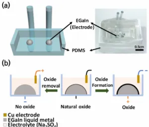
Fig. 1. (a) Experimental setup of a EGaIn capacitor. (b) Electro-
chemical process for removal or formation of the oxide layer on EGaIn electrodes by bias application는 전기이중층 커패시터 (electric double-layer capaci- tor, EDLC)와 전기화학 반응을 동반한 유사커패시터 (pseudocapacitor) 그리고 두 매커니즘을 접목시킨 하 이브리드 커패시터 등으로 분류된다.
최근 갈륨계 액체금속을 초유연 신축 소자의 전극 물질로 응용하고자 하는 연구가 진행되고 있다
1-7). 대표 적인 갈륨계 액체금속은 갈륨과 인듐의 공융 (eutectic) 조성 합금인 eutectic gallium-indium (EGaIn)과 갈륨- 인듐-주석 합금인 Galinstan이 있다. 이들 갈륨계 합 금은 녹는점이 낮아 (갈륨: ~29.7°C, EGaIn: ~15.5°C
8), Galinstan: ~-19°C
9)) 상온에서 액체 상태로 존재하 며 금속의 높은 전기전도도를 가지고 있다(갈륨:
3.7×10
6S/m, EGaIn: 3.4×10
3S/m
10), Galinstan:
3.46×10
6S/m
11)). 특히 갈륨계 액체금속은 다른 액체 금속들에 비하여 독성이나 반응성이 낮아 상대적으 로 안전하다
12). 예를 들어 대표적인 액체금속인 수은 은 독성이 높으며 , 라듐과 세슘은 반응성이 매우 커 서 응용에 제약이 따른다 . 갈륨계 액체금속은 이러한 문제점이 적기 때문에 전자소자, 센서, 약물 전달 등 의 다양한 응용분야에서 주목을 받고 있다
13-15).
갈륨계 액체금속의 또 다른 중요한 특징은 표면에 수 나노미터 두께의 갈륨 산화막을 자발적으로 형성 하는 것이다
16-19). 표면장력이 높아 성형이 어려운 수 은과 달리, 갈륨계 액체금속은 표면에 형성된 자연산 화막 (native oxide)이 표면장력을 낮추어 주기 때문에 구형 외에 다양한 모양 구현이 가능하다
20-27). 이 산 화막은 밴드갭이 커서 (E
g: ~5 eV
28)) 전기적으로는 부 도체이다. 그러므로 나노 절연막이 표면에 형성된 갈 륨계 액체금속은 전하 전달 반응이 억제된 이상 분 극 전극(ideally polarizable electrode)에 가까운 특성 을 띄어 전기이중층 커패시터와 유사한 거동을 보일 수 있다
29). 본 논문에서 우리는 두 개의 EGaIn 전극 과 전해질을 기반으로 커패시터(이하 EGaIn 커패시 터)를 구성하고, 여기서 나타나는 커패시터 거동 분 석 결과를 발표한다. 먼저, cyclic voltammetry (CV) 실험을 통하여 EGaIn 커패시터가 전기이중층 커패 시터의 충방전 거동 특성을 보임을 확인한다. 산화막 두께가 커패시터 거동에 미치는 영향을 보기 위하여 ,
산화/환원 과전압을 이용하여 EGaIn 산화막의 두께 를 조절하고 그에 따른 커패시턴스값 변화를 살펴본 다. 그리고 산화막이 제거된 EGaIn 전극에서 반복 충방전 과정 동안 산화막이 자발적 복구되는 독특한 자기복구(self-repair) 특성에 대하여 논의한다. 마지 막으로 , 전해질 농도의 영향을 살피기 위하여 전해질 의 농도를 달리하여 CV 그래프와 커패시턴스값을 비교한다.
2. 실 험
EGaIn 전극기반 커패시터(이하 EGaIn 커패시터) 의 전기화학 특성 분석을 위하여 , Fig. 1(a)와 같은 장 치를 구성하였다 . 먼저, polydimethylsiloxane (PDMS) 로 사각 틀을 만들고, 바닥에 두 개의 구멍을 뚫어, 지름 500 μm의 타이곤 튜브를 연결한다. 두 개의 튜 브에 각각 EGaIn (Sigma-Aldrich)을 주입하여 EGaIn 전극을 만들고 전해질을 채운다. 전해질은 황산나트 륨(Na
2SO
4, Sigma-Aldrich) 용액을 사용하였다. 결과 적으로 본 전기화학 시스템은 EGaIn/전해질(Na
2SO
4)/
EGaIn 계면으로 구성된다. CV 실험은 전기화학분석
시스템(EIS system, Bio-logic, SP-200)을 사용하여,
-0.3에서 0.3 V 범위에서 주사속도를 50-500 mV/s로
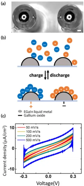
Fig. 2. (a) A top-view image of the EGaIn liquid metal electro-
des of the EGaIn capacitor. Scale bar=0.5 mm. (b) Charging- discharging mechanism of the EGaIn capacitor. (c) CV curves of the EGaIn capacitor with native oxide at different sweep rates. 1 M of Na2SO4 aqueous solution was used as electrolyte달리하며 측정하였다 . 커패시턴스는 CV 그래프로부 터 아래 식을 이용하여 계산하였다
30).
I, ν, ΔV는 각각 전류, 전압주사속도, 주사 전압 범위 이다.
갈륨 산화막의 유무와 두께가 EGaIn 커패시터의 전기화학 특성에 미치는 영향을 알아보기 위해서 , Fig. 1(b)와 같이 산화/환원 과전압을 이용하여, 산화 막을 제거 또는 추가 형성하였다 . 전해질에 잠긴 EGaIn 액체금속 한쪽에 전극을 연결하고 다른 한쪽 역시 전해질에 담겨진 구리선 전극에 연결한다 . EGaIn에 음의 과전압(환원 과전압)을 가해주면 산화 막이 환원되면서 점차 제거되고, 양의 과전압(산화 과전압)을 걸어주면 추가 산화가 진행되면서 산화막 이 더욱 두꺼워지게 된다.
3. 결과 및 고찰
실제 제작한 EGaIn 커패시터의 전극의 모습은 Fig. 2(a)에 나와 있다. 균일한 두께의 나노절연막이 자발적으로 형성되어 거울면과 같은 표면 morphol- ogy를 관찰할 수 있다. Fig. 2(b)에서 보듯이, EGaIn 커패시터의 작동 매커니즘은 일반적인 EDLC와 거 의 유사하다 . 산화막이 있는 EGaIn 전극에 충전 전 압을 가하면 전해질 내에 있는 이온들이 나노 절연 산 화막 위에 쌓이면서 충전이 되고 , 방전 시에는 쌓여있 던 이온들이 풀리면서 전류를 발생시킨다 . EGaIn 커 패시터의 특성을 알아보기 위하여 -0.3에서 0.3 V의 전압 범위에서 CV 곡선을 측정하였다(Fig. 2[c]). 이 론적으로 EDLC는 직사각형의 CV 곡선을 보여주는 데, EGaIn 커패시터의 CV 결과 그래프는 기울어진 직사각형의 모양으로 EDLC와 유사한 거동을 보여주 고 있다 . 주사속도에 비례해서 CV 곡선의 면적도 넓어 지는데 이는 EDLC의 전형적인 CV 특성이다
31). 제작된 EGaIn 슈퍼커패시터는 500 mV/s일 때 ~8.4 mF/cm
2의 커패시턴스를 가지고 있다 . 이처럼, 갈륨 나노 산화막 을 가지고 있는 두 개의 EGaIn 대칭 전극과 전해질로 구성된 EGaIn 커패시터는 일반적인 EDLC 거동을 보여준다.
EGaIn 전극의 표면 산화막의 두께가 EGaIn 커패
시터의 특성에 미치는 영향을 관찰하기 위하여 산화
막의 두께를 조절하여 CV 측정을 하였다. EGaIn의
갈륨 산화막의 두께는 EGaIn에 충방전 측정전압인
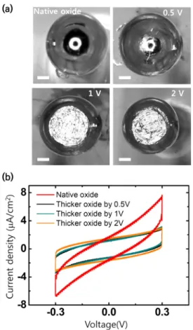
Fig. 3. (a) Top-view images of EGaIn liquid metal electrodes
after further oxidation with different oxidative voltages. Scale bar=0.5 mm. Each oxidative voltage was applied for 30 s. (b) CV curves of the capacitors with the EGaIn electrodes in (a).The scan rate is 200 mV/s
Fig. 4. Stability of the EGaIn capacitors depending on the
thickness of oxide layer. (a) CV curves of the oxide-free EGaIn capacitor during 200 cycles. (b) Comparison of CV curve of the oxide-free EGaIn capacitor at 200th cycle, to that of the EGaIn capacitor with the native oxide at the first cycle. (c) CV curve of the EGaIn capacitor with thicker oxide by 1 V0.3 V 이상의 높은 과전압을 가하여 조절하였다
32-34). 산화 전압인 양의 과전압을 가해주면 자연 산화막이 더욱 두꺼워지고 , 반대로 환원 전압인 음의 과전압을 가해주면 산화막이 제거된다. Fig. 3(a)는 가해준 산 화 과전압의 세기에 따른 EGaIn 전극 표면의 mor- phology 변화를 보여준다. 산화 과전압이 증가함에 따라, 주름이 생기는 등 표면의 morphology 변화가 크게 나타나는데, 이는 표면 산화막이 점점 두꺼워짐 에 따른 결과로 볼 수 있다
33). Fig. 3(b)에서 EGaIn 전극의 갈륨 산화막 두께에 따른 EGaIn 커패시터의 CV 특성을 비교하였다. 자연 산화막을 가진 EGaIn 전극의 경우(13.3 mF/cm
2)와 비교해보면, 0.5 V 이상 의 산화 전압에 의하여 두꺼운 산화막이 형성된
EGaIn 전극의 경우(6.4-7.5 mF/cm
2) 커패시턴스가 절반 정도로 감소하였다. 이는 두꺼워진 산화막에서 전압 손실이 커졌기 때문으로 보인다 . 그러나 0.5 V 이상의 산화 과전압 조건에서는 산화전압의 크기와 무관하게 거의 유사한 CV 그래프 경향을 보였으며, 그 결과 커패시턴스값도 거의 일정하게 유지되었다 .
EGaIn 금속 표면에 형성되는 갈륨 산화막은 EGaIn
Fig. 5. Capacitance for 200 cycles at difference oxide thickness.
The scan rate is 500 mV/s
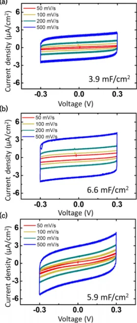
Fig. 6. Effect of electrolyte concentrations on CV curves of
EGaIn based capacitors; (a) 0.01 M, (b) 0.1 M, (c) 1 M. For the stable CV measurement, oxide skin was further oxidized un- der 1 V for 30 seconds. Aqueous Na2SO4 solutions were used as the electrolyte커패시터의 EDLC 거동 특성 메커니즘에서 중요한 역할을 한다. 이러한 산화막의 필요성을 확인하기 위 하여 산화막을 제거한 EGaIn을 전극으로 하여 연속 적으로 CV 측정을 하였다(Fig. 4[a]). 첫 번째 CV 사 이클에서 절연막 역할을 하는 산화막이 없기 때문에 , 전기이중층 형성에 의한 충 /방전보다는 전압에 따른 산화/환원 반응이 우세하게 발생하여 전류는 높게 나 타나지만 EDLC의 전형적인 직사각형 CV 그래프에 서는 많이 벗어난 그래프 모양을 보여준다 . 사이클이 진행됨에 따라 전류가 지속 감소되는데 , 이는 열역학 적으로 자발적인 EGaIn 산화 반응에 의하여 갈륨 산 화막이 지속적으로 형성되기 때문일 것이다. 연속 CV 사이클을 거치는 동안, Fig. 4(a)에서 보이는 것 과 같이 수평으로 누운 형태의 그래프로 점점 변화하 게 된다. 산화막이 제거된 EGaIn 커패시터를 200회 의 CV 사이클을 거친 후 CV 그래프를 산화막이 제 거되지 않은 EGaIn 커패시터와 비교해보면, 유사한 그래프 모양을 보인다(Fig. 4[b]). 그에 비하여 1 V 산화 과전압에 의하여 형성된 산화막을 가지고 있는 EGaIn전극은 충방전이 계속될 때에도 직사각형의 그래프모양을 거의 일정하게 유지하고 있는 것을 Fig. 4(c)에서 확인할 수 있다.
Fig. 5는 각 산화막 상태에서의 면적 당 커패시턴 스를 사이클 횟수에 따라 나타냈다. 충방전 사이클이 진행될수록 , oxide-free EGaIn 전극 조건에서는 커패 시턴스값이 55.3 mF/cm
2에서 200번째 사이클에서는
11.5 mF/cm
2로 5배 정도 감소하는 것을 볼 수 있다.
이 값은 자연산화막을 가진 EGaIn 전극의 커패시턴
스값인 8.4 mF/cm
2에 가까워진다 . 1 V에 의하여 두
꺼운 산화막이 형성된 EGaIn의 커패시터의 경우, 커
패시턴스값은 200사이클 동안 3.7-3.8 mF/cm
2로 거
의 일정하게 유지되며 가장 높은 작동 안정성을 보 여준다. 이상 EGaIn 커패시터의 면적당 커패시턴스 값은 기존에 보고된 탄소기반 전기이중충 커패시터들 의 수치와 비교해볼 때, 비슷하거나 10배 더 나은 값
이다
35-37). 이처럼, 갈륨 산화막을 가지고 있는 EGaIn
기반 커패시터는 연속적인 충방전 사이클에도 안정 적인 성능을 보여준다 . 또한, 갈륨 산화막이 제거된 EGaIn 전극의 경우, 충방전 사이클을 거치면서 자발 적으로 산화막이 재생되는 독특한 자기복구 (self-re- pair) 특성을 보임을 알 수 있다.
전해질 농도에 따른 커패시턴스 차이를 보기 위 하여 전해질의 농도를 0.01, 0.1, 1 M로 달리하여 CV 분석을 진행하였다(Fig. 6). 커패시턴스의 값은 500 mV/s 기준으로 0.01 M일 때 3.9 mF/cm
2, 0.1 M 일 때 6.6 mF/cm
2, 1 M일 때 5.9 mF/cm
2로 계산되었 다. 전해질의 농도가 0.01 M에서 0.1 M로 증가함에 따라 커패시턴스가 증가하는 반면, 0.1 M에서 1 M 로 증가할 때는 커패시턴스값에 큰 변화가 없고 오 히려 소폭 감소하였다 . 이는 1 M일 때 이온의 농도 가 과도하게 높아져 이온들끼리 간섭현상이 일어난 것으로 추정된다. 이상의 결과를 바탕으로, 본 실험 에 사용된 EGaIn 커패시터 조건에서는 약 0.1 M의 전해질 농도에서 가장 높고 안정된 EDLC 거동을 보 임을 알 수 있다.
4. 결 론
본 논문에서는 액체금속 EGaIn 전극을 기반으로 EDLC 커패시터를 제작하였다. 표면에 형성되는 갈 륨 산화막에 전기 이중층이 효과적으로 형성되어 커 패시터 특성을 보이는 것을 확인하였다 . EGaIn 산화 막 두께를 달리하며 CV 그래프를 비교해본 결과, 자 연산화막 이상으로 두꺼워진 산화막은 충방전 전류 및 커패시턴스를 감소시킴을 확인하였다 . 갈륨 산화 막이 제거된 EGaIn 전극을 이용한 커패시터의 경우, CV 그래프의 전류는 높지만 전형적인 EDLC 거동에 서 다소 벗어난 CV 그래프를 보였다. 산화막이 제거 된 EGaIn 전극의 경우, 연속 충방전 사이클을 거치
면서 산화막이 자발적으로 형성되는 자기복구 특성 을 관찰할 수 있었다 . 자연산화막 이상의 두꺼운 산 화막이 존재할 때는 EGaIn 커패시터의 커패시턴스 값은 약간 저하되지만, 반복측정에도 커패시터값이 거의 일정하게 유지되어 우수한 작동 안정성을 보여 주었다. 0.01-1 M 범위에서 전해질 농도를 달리하며 EGaIn 커패시터의 CV 측정을 해본 결과, ~0.1 M에 서 가장 높고 안정적인 성능을 보였다. 이상의 연구 결과는 EGaIn 액체금속을 이용한 전기화학 에너지 소자 개발 연구에 중요한 정보를 제공할 수 있을 것 이다.
후 기
본 연구는 서울과학기술대학교 교내연구비의 지 원으로 수행되었다 .
References
1. M. Varga, C. Ladd, S. Ma, J. Holbery, and G. Trsöter,
“On-skin liquid metal inertial sensor”, Lab on a Chip, Vol.
17, No. 19, 2017, pp. 3272-3278.
2. X. Shi, C. H. Cheng, Y. Zheng, and P. Wai, “An egain-based flexible piezoresistive shear and normal force sensor with hysteresis analysis in normal force direction”, Journal of Micromechanics and Microengineering, Vol. 26, No. 10, 2016, p. 105020.
3. H. Ota, K. Chen, Y. Lin, D. Kiriya, H. Shiraki, Z. Yu, T. J. Ha, and A. Javey, “Highly deformable liquid-state hetero- junction sensors”, Nature Communications, Vol. 5, 2014, p.
5032.
4. J. B. Chossat, Y. L. Park, R. J. Wood, and V. Duchaine, “A soft strain sensor based on ionic and metal liquids”, IEEE Sensors Journal, Vol. 13, No. 9, 2013, pp. 3405-3414.
5. Y. Gao, H. Ota, E. W. Schaler, K. Chen, A. Zhao, W. Gao, H.
M. Fahad, Y. Leng, A. Zheng, F. Xiong, C. Zhang, L. C. Tai, P. Zhao, R. S. Fearing, and A. Javey, “Wearable microfluidic diaphragm pressure sensor for health and tactile touch monitoring”, Advanced Materials, Vol. 29, No. 39, 2017, p.
1701985.
6. G. Li, X. Wu, and D. W. Lee, “A galinstan-based inkjet print- ing system for highly stretchable electronics with self-heal- ing capability”, Lab on a Chip, Vol. 16, No. 8, 2016, pp.
1366-1373.
7. A. Tabatabai, A. Fassler, C. Usiak and C. Majidi, “Liquid- phase gallium-indium alloy electronics with microcontact printing”, Langmuir, Vol. 29, No. 20, 2013, p. 6194.
8. M. D. Dickey, R. C. Chiechi, R. J. Larsen, E. A. Weiss, D. A.
Weitz, and G. M. Whitesides, “Eutectic gallium-indium (egain): A liquid metal alloy for the formation of stable structures in microchannels at room temperature”, Advanced Functional Materials, Vol. 18, No. 7, 2008, pp.
1097-1104.
9. T. Liu, P. Sen, and C. J. Kim, “Characterization of nontoxic liquid-metal alloy galinstan for applications in micro- devices”, Journal of Microelectromechanical Systems, Vol.
21, No. 2, 2012, pp. 443-450.
10. D. Zrnic and D. S. Swatik, “On the resistivity and surface tension of the eutectic alloy of gallium and indium”, Journal of the Less Common Metals, Vol. 18, No. 1, 1969, pp. 67-68.
11. C. Karcher, V. Kocourek, and D. Schulze, “Experimental in- vestigations of electromagnetic instabilities of free surfaces in a liquid metal drop”, International Scientific Colloquium, Modelling for Electromagnetic Processing, 2003, pp. 105-110.
12. J. H. Kim, S. Kim, J. H. So, K. Kim, and H. J. Koo,
“Cytotoxicity of Gallium–Indium Liquid Metal in Aqueous Environment”, ACS Applied Materials & Interfaces, Vol.
10, No. 20, 2018, pp. 17448-17454.
13. Y. Lu, Q. Hu, Y. Lin, D. B. Pacardo, C. Wang, W. Sun, F. S.
Ligler, M. D. Dickey, and Z. Gu, “Transformable liq- uid-metal nanomedicine”, Nature Communications, Vol.
6, 2015, p. 10066.
14. J. E. Chandler, H. H. Messer, and G. Ellender, “Cytotoxicity of gallium and indium ions compared with mercuric ion”, Journal of Dental Research, Vol. 73, No. 9, 1994, pp.
1554-1559.
15. R. C. Chiechi, E. A. Weiss, M. D. Dickey, and G. M.
Whitesides, “Eutectic gallium-indium (egain): A moldable liquid metal for electrical characterization of self-as- sembled monolayers”, Angewandte Chemie International Edition, Vol. 47, No. 1, 2007, pp. 142-144.
16. A. J. Downs, “Chemistry of aluminium, gallium, indium and thallium”, Vol. 1, Springer, the Netherlands, 1993.
17. J. Thelen, M. D. Dickey, and T. Ward, “A study of the pro- duction and reversible stability of egain liquid metal micro- spheres using flow focusing”, Lab on a Chip, Vol. 12, No. 20, 2012, pp. 3961-3967.
18. Q. Xu, N. Oudalov, Q. Guo, H. M. Jaeger, and E. Brown,
“Effect of oxidation on the mechanical properties of liquid gallium and eutectic gallium-indium”, Physics of Fluids, Vol. 24, No. 6, 2012, p. 063101.
19. S. Holcomb, M. Brothers, A. Diebold, W. Thatcher, D. Mast,
C. Tabor, and J. Heikenfeld, “Oxide-free actuation of gal- lium liquid metal alloys enabled by novel acidified siloxane oils”, Langmuir, Vol. 32, No. 48, 2016, pp. 12656-12663.
20. Y. Tokuda, J. L. B. Moya, G. Memoli, T. Neate, D. R. Sahoo, S. Robinson, J. Pearson, M. Jones, and S. Subramanian,
“Programmable liquid matter: 2d shape deformation of highly conductive liquid metals in a dynamic electric field”, Proceedings of the 2017 ACM International Conference on Interactive Surfaces and Spaces, ACM, 2017, p. 142.
21. S. Zhu, J. H. So, R. Mays, S. Desai, W. R. Barnes, B.
Pourdeyhimi, and M. D. Dickey, “Ultrastretchable fibers with metallic conductivity using a liquid metal alloy core”, Advanced Functional Materials, Vol. 23, No. 18, 2013, pp.
2308-2314.
22. T. Hutter, W. A. C. Bauer, S. R. Elliott, and W. T. Huck,
“Formation of spherical and non spherical eutectic gal- lium-indium liquid metal microdroplets in microfluidic channels at room temperature”, Advanced Functional Materials, Vol. 22, No. 12, 2012, pp. 2624-2631.
23. A. Diebold, A. Watson, S. Holcomb, C. Tabor, D. Mast, M.
Dickey, and J. Heikenfeld, “Electrowetting-actuated liquid metal for rf applications”, Journal of Micromechanics and Microengineering, Vol. 27, No. 2, 2017, p. 025010.
24. A. Fassler and C. Majidi, “3d structures of liquid-phase gain alloy embedded in pdms with freeze casting”, Lab on a Chip, Vol. 13, No. 22, 2013, pp. 4442-4450.
25. Y. Zheng, Z. Z. He, J. Yang, and J. Liu, “Personal electronics printing via tapping mode composite liquid metal ink de- livery and adhesion mechanism”, Scientific Reports, Vol. 4, 2014, p. 4588.
26. C. Ladd, J. H. So, J. Muth, and M. D. Dickey, “3d printing of free standing liquid metal microstructures”, Advanced Materials, Vol. 25, No. 36, 2013, pp. 5081-5085.
27. J. W. Boley, E. L. White, G. T. C. Chiu, and R. K. Kramer,
“Direct writing of gallium-indium alloy for stretchable electronics”, Advanced Functional Materials, Vol. 24, No.
23, 2014, pp. 3501-3507.
28. Y. S. Lee, D. Chua, R. E. Brandt, S. C. Siah, J. V. Li, J. P.
Mailoa, S. W. Lee, R. G. Gordon, and T. Buonassisi, “Atomic layer deposited gallium oxide buffer layer enables 1.2 v open circuit voltage in cuprous oxide solar cells”, Advanced Materials, Vol. 26, No. 27, 2014, pp. 4704-4710.
29. J. So and H. J. Koo, “Study on the Electrochemical Characteristics of a EGaIn Liquid Metal Electrode for Supercapacitor Applications”, Trans. of the Korean Hydrogen and New Energy Society, Vol. 27, No. 2, 2016, pp.
176-181.
30. M. D. Stoller and R. S. Ruoff, “Best practice methods for de- termining an electrode material's performance for ultra- capacitors”, Energy & Environmental Science, Vol. 3, No. 9,
2010, pp. 1294-1301.
31. L. R. F. Allen J. Bard, “Electrochemical methods funda- mentals and applications”, Willey, USA, 2001.
32. J. H. So, H. J. Koo, M. D. Dickey, and O. D. Velev, “Ionic cur- rent rectification in soft matter diodes with liquid metal electrodes”, Advanced Functional Materials, Vol. 22, No. 3, 2012, pp. 625-631.
33. H. J. Koo, J. H. So, M. D. Dickey, and O. D. Velev, “Towards all soft matter circuits: Prototypes of quasi liquid devices with memristor characteristics”, Advanced Materials, Vol.
23, No. 31, 2011, pp. 3559-3564.
34. M. R. Khan, C. B. Eaker, E. F. Bowden, and M. D. Dickey,
“Giant and switchable surface activity of liquid metal via surface oxidation”, Proceedings of the National Academy of Sciences, Vol. 111, No. 39, 2014, pp. 14047-14051.
35. D. Membreno, L. Smith, K. S. Shin, C. O. Chui, and B.
Dunn, “A high-energy-density quasi-solid-state carbon nanotube electrochemical double-layer capacitor with ion- ogel electrolyte”, Translational Materials Research, Vol. 2, No. 1, 2015, p. 015001.
36. Y. Q. Jiang, Q. Zhou, and L. Lin, “Planar mems super- capacitor using carbon nanotube forests”, 2009 IEEE 22nd International Conference on Micro Electro Mechanical Systems, 2009, pp. 587-590.
37. D. Pech, M. Brunet, P.-L. Taberna, P. Simon, N. Fabre, F.
Mesnilgrente, V. Conédéra, and H. Durou, “Elaboration of a microstructured inkjet-printed carbon electrochemical capacitor”, Journal of Power Sources, Vol. 195, No. 4, 2010, pp. 1266-1269.