http://dx.doi.org/10.5369/JSST.2015.24.1.15 pISSN 1225-5475/eISSN 2093-7563
Electrical and Optical Properties of Asymmetric Dielectric/Metal/Dielectric (D/M/D) Multilayer Electrode Prepared by Radio-Frequency Sputtering for Solar Cells
Rina Pandey
1,2, Ju Won Lim
1, Keun Yong Lim
1, Do kyung Hwang
1,2, and Won Kook Choi
1,2,+Abstract
Transparent and conductive multilayer thin films consisting of three alternating layers FZTO/Ag/WO
3have been fabricated by radio- frequency (RF) sputtering for the applications as transparent conducting oxides and the structural and optical properties of the resulting films were carefully studied. The single layer fluorine doped zinc tin oxide (FZTO) and tungsten oxide (WO
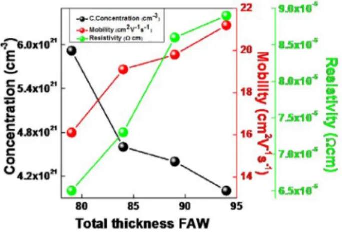
3) films grown at room tem- perature are found to have an amorphous structure. Multilayer structured electrode with a few nm Ag layer embedded in FZTO/Ag/
WO
3(FAW) was fabricated and showed the optical transmittance of 87.60 % in the visible range (λ = 380~770 nm), quite low electrical resistivity of ~ 10
-5Ω cm and the corresponding figure of merit (T
10/R
s) is equivalent to 3.0×10
-2Ω
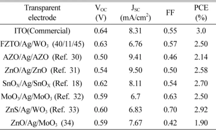
-1. The resultant power conversion efficiency of 2.50% of the multilayer based OPV is lower than that of the reference commercial ITO. Asymmetric D/M/D multilayer is a promising transparent conducting electrode material due to its low resistivity, high transmittance, low temperature deposition and low cost components.
Keywords: Transparent conductive oxide, RF Sputtering, Structural and optical properties, Bulk hetero-junction organic pho- tovoltaic’s cells (BHJ-OPVs), Power conversion efficiency
1. INTRODUCTION
Transparent conducting oxides (TCO) are the integral part of the present day electro-optic devices as transparent conducting electrode (TCE). The inherent properties, transmittance and electrical conductivity of the TCOs are important factors which make them potential candidates for TCE applications such as plasma display panels, flat panel displays, touch panels, solar cells, organic light emitting diode, and gas sensors [1]. Different metal oxide semiconductors like In 2 O 3 , SnO 2 , ZnO, and TiO 2 have been extensively employed to fabricate TCO thin films [2]. The most common TCO consists of large band gap semiconducting metal oxides such as indium, tin, cadmium and zinc oxide doped with group III (Al [3-7], B [8], Ga [9-11] or group VII (F [12], Cl
[13] elements to reduce their resistivity while retaining high transparency in the visible range (λ=380~770 nm). Because of high conductivity, transparency, and the possibility to generate very flat films with good reproducibility, indium tin oxide (ITO) is one of the most employed TCO [14]. Due to the high cost and scarcity of indium in TCO, there is urgent need of an alternative material with low cost and similar properties [2]. In these days, researchers are dedicated to find new transparent conductive electrodes such as nanotubes, graphene, metal nanowires, dielectric-metal-dielectric (D/M/D) and related structures. D/M/D materials have been suggested as a candidate to overcome the limits of both the electrical and optical properties of single layer TCOs. It allows both the overall carrier concentration and the mobility to be increased, prevailing to some extent the limitation imposed by ionized impurity scattering in metal oxide single layers. Sandwiching a thin metal layer between two dielectric layers D/M/D has been presented as an alternative approach to obtain the combined benefits of high transmission as well as the excellent conductivity of metals. Studies on a variety of multilayer electrodes [15-22] have been investigated for indium free transparent conducting oxides for organic photovoltaic’s cells.
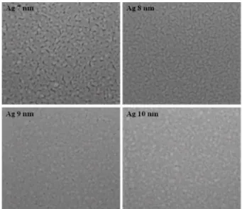
Silver was found to perform the best as the middle metal layer in sandwiched D/M/D structure. A pure Ag metal film has the lowest resistivity of all metals and exhibits relatively low absorption in the visible region. In our study, Fluorine doped zinc tin oxide
1
Interface Control Research Center, Korea Institute of Science and Technology (KIST), Seongbuk Gu, Hwarangro 14 Gil 5, Seoul 136-791, Korea
2
Department of Nanomaterials Science and Engineering, Korea University of Science and Technology (KUST), Gajeongro 217, Yuseong-gu, Daejeon 305- 350, Korea
+