DOI: http://dx.doi.org/10.4313/JKEM.2016.29.7.387 ISSN 1226-7945 (Print), 2288-3258 (Online)
박막트랜지스터의 병렬형 가역과 비가역 문턱전압 이동에 대한 모델링
정태호a
서울과학기술대학교 전자공학과
Modeling of Reversible and Irreversible Threshold Voltage Shift in Thin-film Transistors
Taeho Jung
aDepartment of Electronics Engineering, Seoul National University of Science and Technology, Seoul 01811, Korea
(Received May 17, 2016; Revised June 16, 2016; Accepted June 17, 2016)
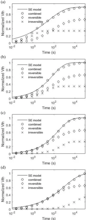
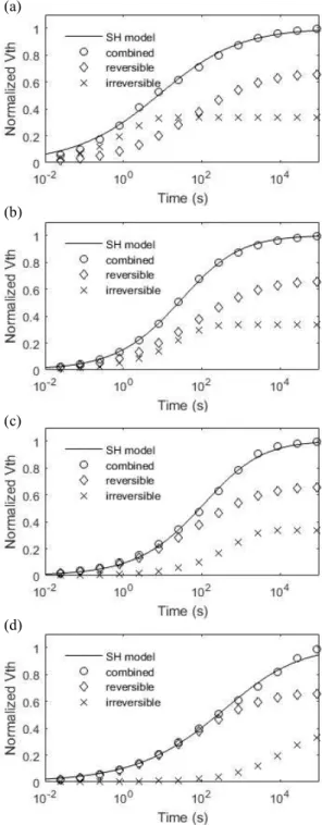
Abstract: Threshold voltage shift has been observed from many thin-film transistors (TFTs) and the time evolution
of the shift can be modeled as the stretched-exponential and -hyperbola function. These analytic models are derived from the kinetic equation for defect-creation or charge-trapping and the equation consists of only reversible reactions. In reality TFT’s a shift is permanent due to an irreversible reaction and, as a result, it is reasonable to consider that both reversible and irreversible reactions exist in a TFT. In this paper the case when both reactions exist in parallel and make a combined threshold voltage shift is modeled and simulated. The results show that a combined threshold voltage shift observed from a TFT may agrees with the analytic models and, thus, the analytic models don’t guarantee whether the cause of the shift is defection-creation or charge-trapping.Keywords: Threshold voltage shift, Thin-film transistor, Kinetic equation
1. 서 론
박막 트랜지스터(thin-fim transistor, TFT)는 일반 적으로 저온제작 공정과 재료의 특성으로 인해 단결정 실리콘 트랜지스터에 비해 전하 캐리어의 이동도가 낮 으며, 동작 전압과 온도, 시간에 따라 전기적 특성이 변하는 등의 단점을 갖고 있다 [1-3]. 이 단점들 중에 서 TFT에 동작 전압이 인가 된 후 받게 되는 스트레
a. Corresponding author; [email protected]
Copyright ©2016 KIEEME. All rights reserved.
This is an Open-Access article distributed under the terms of the Creative Commons Attribution Non-Commercial License (http://creativecommons.org/licenses/by-nc/3.0) which permits unrestricted non-commercial use, distribution, and reproduction in any medium, provided the original work is properly cited.
스로 인해 시간에 따라 문턱전압이 이동(threshold
voltage shit, ΔV
t) 하는 현상은 회로의 신뢰성과 관련
되어 있으므로 TFT의 응용분야의 확장에 가장 큰 문
제가 된다. 다양한 TFT들에서 공통적으로 관측되는 Δ
V
t현상을 설명하는 연구는 주로 비정질 실리콘 박막
트랜지스터 (amorphous silicon TFT, a-Si TFT)를
대상으로 진행되었으며, 이 결과에 따른 TFT의 응답은
분석 모델로 제작되었다 [4]. a-Si TFT에서 관측되는
ΔV
t현상은 반도체 채널 내에서의 결함생성과 게이트
절연체로의 전하포획 현상으로 설명되었다. 전자의 경
우에 시간에 따라 ΔV
t가 변하는 모양은 stretched
exponential (SE) 또는 stretched hyperbola (SH)
형태의 분석적 수식으로 유도되었다 [5,6].
∆
∞
∆