1. 서 론
전차선로 설비에서 가장 중요한 재료는 전기절연재료 인 자기애자이다. 자기애자의 경우 우수한 절연특성을 가지고 있지만, 무겁고 내충격에 대한 결함 때문에 파괴 되기 쉬우며 취급에 많은 어려움을 가지고 있다. 전기철 도 분야에서는 이러한 자기애자의 단점을 해결하고자, 우수한 내오손성을 지니며 가벼운 고분자 애자의 사용 량을 증대시키고 있다. 전 세계적으로도 고분자(폴리머) 애자의 사용량은 증가되고 있지만, 고분자 애자 역시 재
✉ Yong Seob Park; [email protected] Copyright ©2021 KIEEME. All rights reserved.
This is an Open-Access article distributed under the terms of the Creative Commons Attribution Non-Commercial License (http://creativecommons.org/licenses/by-nc/3.0) which permits unrestricted non-commercial use, distribution, and reproduction in any medium, provided the original work is properly cited.
질의 고유한 특성 때문에 자기 애자보다 분진 등 오염 원의 부착이 쉽게 이루어지며, 세척이 매우 어려운 단점 을 지니고 있다. 장기적인 관점에서 고분자 애자를 직류 전기철도 분야에 사용하기 위해서는 고분자 애자의 고 유 절연 특성이 변하지 않도록 내오손성을 지니고 내아 크성의 장점을 지니며, 세척을 쉽게 할 수 있도록 해야 한다 [1]. 본 연구에서는 고분자 애자의 단점을 해결하 고자 자연 세척과 전기적 절연특성을 유지할 수 있는 방안으로 광촉매 소재를 표면처리 부분에 사용한 환경 기술을 제안하고자하며, 환경 정화기술로써 광촉매 기술 은 빛을 받아 별도의 에너지 없이 유해 유기물을 분해 하여 다른 오염물질을 제거하는 기술로써, 세균을 포함 한 오염물질과 유해한 잔류물들을 완전히 제거하는 방 법이다 [2,3]. 일반적으로 광촉매 소재로는 TiO2, SiO2, WO3, ZnO, CdS 등을 사용하고 있으며, 본 연구에서는
DLC 박막이 코팅된 폴리머 애자의 표면 및 물리적 특성
김영곤, 박용섭
조선이공대학교 전자과
Surface and Physical Properties of Polymer Insulator Coated with Diamond-Like Carbon Thin Film
Young Gon Kim and Yong Seob Park
Department of Electronics, Chosun College of Science & Technology, Gwangju 61453, Korea
(Received September 27, 2020; Revised October 15, 2020; Accepted October 17, 2020)
Abstract: In this study, we tried finding new materials to improve the stain resistance properties of polymer insulating materials. Using the filtered vacuum arc source (FVAS) with a graphite target source, DLC thin films were deposited on silicon and polymer insulator substrates depending on their thickness to confirm the surface properties, physical properties, and structural properties of the thin films. Subsequently, the possibility of using a DLC thin film as a protective coating material for polymer insulators was confirmed. DLC thin films manufactured in accordance with the thickness of various thin films exhibited a very smooth and uniform surface. As the thin film thickness increased, the surface roughness value decreased and the contact angle value increased. In addition, the elastic modulus and hardness of the DLC thin film slightly increased, and the maximum values of elastic modulus and hardness were 214.5 GPa and 19.8 GPa, respectively.
In addition, the DLC thin film showed a very low leakage current value, thereby exhibiting electrical insulation properties.
Keywords: Diamond-like carbon, Filtered vacuum arc source, Contact angle, Hardness, Surface roughness
DOI: https://doi.org/10.4313/JKEM.2021.34.1.16
ISSN 1226-7945(Print), 2288-3258(Online)
이러한 일반적 광촉매 소재가 아닌 다이아몬드상 탄소 (diamond like carbon, DLC) 박막을 광촉매 소재로 사용하고자 한다. DLC의 경우 표면에 대한 친수성과 소수성을 조절할 수 있으며, 가시광 또는 자외선에서 에 너지 밴드갭을 조절할 수 있고, 또한 산과 염기 등에 대해 화학적 안정성을 지니는 장점을 가진다. 본 연구에 서는 DLC 박막을 제작하기 위해 여과된 진공 아크 (FVAS) 장치를 사용하였으며, 이 장치의 경우 다이아몬 드상 탄소(DLC) 또는 사면체 비정질 탄소(ta-C) 박막을 제작할 수 있는 장점을 지니며, 특히 높은 이온 에너지 와 이온화 비율로 밀도가 높은 비정질 탄소 박막을 제 작하는 데 장점을 지니고 있다 [4-6].
FVAS 장치를 이용하여 실리콘과 고분자 폴리머 애 자 기판 위에 DLC 박막을 증착하였으며, 증착된 DLC 박막의 표면 특성, 물리적 특성, 구조적⋅전기적 특성 등을 분석하고 이 특성들 사이에 상관관계를 고 찰하였다.
2. 실험 방법
다이아몬드형 탄소(DLC) 박막은 흑연 타깃(음극) 소스를 이용한 여과된 진공아크(filtered vacuum arc source, FVAS)를 사용하여 (100) p형 실리콘 기판과 폴리머애 자 기판상에 증착하였다. DLC 필름을 증착 전 모든 기판들은 아세톤, 메탄올 및 탈 이온수 등 각 용액에 서 10분 동안 세척하였다. DLC 박막을 증착하기 위한 기본 압력과 증착 압력은 각각 5×10⁻⁵ Torr와 2×10⁻³ Torr로 설정하였다. 버퍼 챔버의 아르곤 가스의 유량 은 25 sccm으로 일정하게 유지하였고, DLC 박막을 위한 바이어스 전압은 약 131 V이고 DLC 박막의 증착 온도는 30℃로 설정하였다. DLC 박막의 두께는 증착시 간을 달리하여 제작하였으며, 시간은 각각 8분에서 17 분까지 각각 3분 간격으로 증착하였다. 본 연구에서는 실리콘과 폴리머애자 기판 상에 다양한 두께로 증착된 DLC 박막의 표면과 물리적 특성들을 측정, 고찰하였 다. 모든 막의 두께 및 표면 형태는 전계 방출주사전자 현미경(FESEM: Hitachi, S-4700) 및 surface testing platform (Nanosystem, Anton, STeP6)을 사용하여 측정되었고, 구조적 특성은 다음을 사용하여 평가되었 다. DLC 필름의 탄성계수와 경도 값은 나노박막 스크 래치 테스터(Anton Paar 사, 스위스)로 측정되었으며, 박막의 표면 에너지는 접촉각 측정(SEO 300 A, 물방 울 3 μL)을 이용하여 측정하였다.
3. 결과 및 고찰
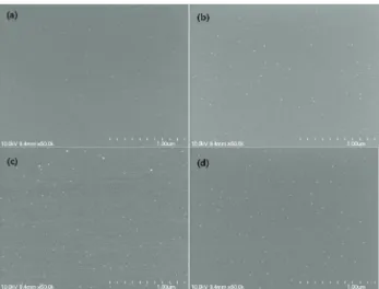
그림 1은 FVAS 장치를 이용하여 두께가 증가함에 따라 제작된 DLC 박막의 FESEM 표면 이미지를 나타 낸다. 그림에서 확인할 있듯이, DLC 두께는 38 A의 아 크 전류에서 박막의 성장 속도가 분당 약 4.3 nm이며, 성장 속도를 기준으로 박막의 두께를 조절하였다. 아크 전류의 크기는 탄소의 이온화 정도의 증가를 나타내며, 아크 전류의 크기는 탄소 이온의 운동 에너지와 관련되 며, 특히 박막 표면에서 이온 이식(ion implantation)과 이온의 재스퍼터링(resputtering)에 기인하게 된다. 본 실험에서는 38 A의 아크 전류가 동일하며, 증착 시간 을 달리하여 박막의 두께를 결정하였기 때문에 FESEM 표면에서는 많은 차이점을 보이지 않았다.
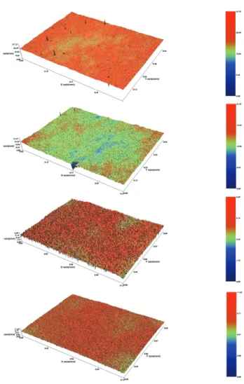
그림 2와 그림 3은 FVAS 장치를 이용하여 두께가 증가함에 따라 제작된 DLC 박막의 표면 거칠기 3D 이 미지와 RMS (root mean squares) 표면 거칠기 값의 변화를 나타낸다. FVAS 장치를 이용하여 증착한 모든 DLC 박막은 매우 매끄럽고 부드러우며, 균일한 표면 거칠기 값을 나타내었고 [6,7], DLC 박막의 두께가 증 가함에 따라 RMS 표면 거칠기 값이 다소 감소하였다.
아크 전류의 크기는 아크 스팟 영역의 크기와 에너지를 얻은 이온들의 이온 이식과 재스퍼터링의 횟수를 결정 하게 된다. 증착시간의 증가는 박막 표면에서 C 및 Ar 이온의 충돌 효과를 증가시키게 되며, 이는 박막의 치 밀도와 표면 거칠기의 감소에 기인하게 된다 [8-10].
그림 4는 FVAS 장치를 이용하여 두께가 증가함에 따
Fig. 1. FESEM surface image of DLC thin film manufactured according to thickness using FVAS.
라 제작된 DLC 박막의 탄성 계수와 경도 값을 변화를 나타낸다. 결과에서 확인할 수 있듯이, DLC 박막의 두
께가 증가함에 따라 탄성계수와 경도 값은 증가하였고, 탄성계수와 경도의 최댓값은 각각 214.5 GPa과 19.8 GPa이었다. DLC 박막의 두께를 증가시키기 위해 증착 시간을 증가시켰는데, 이는 박막이 성장할 때 박막 표면 에서 이온 이식과 이온의 재스퍼터링 효과가 증가하게 된다 [8-11]. 이에 박막은 두께가 증가함에 따라 기판에 인가되는 바이어스 전압에 의해 표면으로 연속적으로 입 사되는 카본 이온들의 충격 열원의 증가 때문에 두께의 증가는 카본 결합력을 증가시키며, 원자 간 결합력이 향 상되어 더욱 치밀해지는 효과가 있으며, 박막의 탄성계 수와 경도가 증가하는 역할을 하게 된다 [12,13].
그림 5~7은 FVAS 장치를 이용하여 두께가 증가함에 따라 폴리머 애자 표면에 증착된 DLC 박막의 표면에 서의 물방울 이미지와 접촉각 이미지, 그리고 접촉각 값의 변화를 나타낸다. 두께가 증가함에 따라 DLC 박 막이 증착된 폴리머 애자의 접촉각 이미지에서 확인할 수 있듯이, DLC 박막의 두께가 증가함에 따라 접촉각 의 이미지와 접촉각의 값은 많은 변화는 보이지 않았 다. 그러나 확실한 결과는 기존 폴리머 애자의 소수 특 성을 더욱 향상시킨 것을 확인할 수 있다. 폴리머 애자 의 접촉각 값은 약 96°를 나타내었으며, FVAS 장치를 이용하여 DLC 박막을 증착한 폴리머 애자의 경우 110° 이상의 초발수 특성을 나타낸 것을 확인하였다.
표면에서 아크 전류와 바이어스 등에 의해 증가된 이온 이식과 이온의 재스퍼터링 효과와 폴리머 애자의 코팅 소재로 사용한 DLC 박막의 결합 특성으로 인해 [5,7], 표면 에너지가 낮은 초발수 특성을 지니는 폴리머 애 자를 제작할 수 있었다. 이는 결합력이 완전한 표면 특성에 기인한다고 할 수 있으며, 폴리머 애자의 내구 성 확보와 오염물질을 제거할 수 있는 기능성 소재로 응용이 가능할 것이라고 판단된다.
20 35 50 65
50 100 150 200 250
Film thickness (nm)
Elastic modulus (GPa)
0 5 10 15 20 25 30 Elastic modulus
Hardness
Hardness (GPa)
Fig. 4. Elastic modulus and hardness value of DLC thin film manufactured according to thickness using FVAS.
Fig. 2. Surface roughness 3D images of DLC thin films fabricated according to thickness using an FVAS.
20 35 50 65
0.0 0.2 0.4 0.6 0.8 1.0 1.2
Rms roughness (nm)
Film thickness (nm)
Fig. 3. Changes in the root mean squares (RMS) surface roughness values of DLC thin films fabricated according to thickness using an FVAS.
4. 결 론
본 연구에서는 흑연 타깃 소스와 함께 FVAS (filtered vacuum arc source) 장치를 이용하여 실리콘과 폴리 머애자 기판에 두께가 증가함에 따라 DLC 박막을 증 착하여 박막의 표면 특성과 물리적 특성, 그리고 구조 특성을 확인하였으며, 또한 전기적 특성을 고찰하여, 폴리머애자의 보호 코팅 소재로서 DLC 박막의 가능성 을 확인하였다. 다양한 박막의 두께가 증가함에 따라 제작된 DLC 박막의 경우 매우 매끄럽고 균일한 표면 을 나타내었으며, 박막의 두께가 증가함에 따라 표면 거칠기 값은 감소하였으며, 접촉각 값은 증가하였다.
또한 DLC 박막의 탄성계수와 경도 값은 다소 증가하 였으며, 그 최댓값은 각각 214.5 GPa과 19.8 GPa을 나타내었다. 또한 전기적으로 DLC 박막은 아주 낮은 누설전류 값을 나타내어 전기적으로 절연 특성을 나타 내는 것을 확인하였다. 이러한 특성들은 박막이 증착되 는 동안 표면에서 아크 전류와 바이어스 등에 의해 증 가된 이온 이식과 이온의 재스퍼터링 효과에 의해 결 합력이 향상되고 결과적으로 부드러운 표면, 낮은 표면 에너지, 그리고 절연 특성을 갖는 DLC 박막을 제작할 수 있었다.
ORCID
Yong Seob Park https://orcid.org/0000-0001-5746-4146
REFERENCES
[1] R. K. Roy and K. R Lee, J. Biomed. Mater. Res., Part B, 83B,
(a) (b)
(c) (d)
Fig. 5. Images of water droplets on the surface of a polymer insulator deposited with DLC of various thicknesses.
Fig. 6. Images of the contact angle measured at the DLC surface on the polymer insulator according to the thickness using the FVAS.
Fig. 7. Change of the contact angle value of the DLC thin film deposited on the surface of the polymer insulator according to the thickness using the FVAS.
Fig. 8. Average leakage current characteristics measured using SPM measurement of devices made of metal-insulator-metal structures.
72 (2007). [DOI: https://onlinelibrary.wiley.com/doi/abs/10.1002/
jbm.b.30768]
[2] T. Hasebe, Y. Matsuoka, H. Kodama, T. Saito, S. Yohena, A.
Kamijo, N. Shiraga, M. Higuchi, S. Kuribayashi, K. Takahashi, and T. Suzuki, Diamond Relat. Mater., 15, 129 (2006). [DOI:
https://doi.org/10.1016/j.diamond.2005.08.025]
[3] J. A. McLaughlin, B. Meenan, P. Maguire, and N. Jamieson, Diamond Relat. Mater., 5, 486 (1996). [DOI: https://doi.org/
10.1016/0925-9635(96)80065-3]
[4] P. D. Maguire, J. A. McLaughlin, T.I.T. Okpalugo, P. Lemoine, P. Papakonstantinou, E. T. McAdams, M. Needham, A. A. Ogwu, M. Ball, and G. A. Abbas, Diamond Relat. Mater., 14, 1277 (2005). [DOI: https://doi.org/10.1016/j.diamond.2004.12.023]
[5] E. Liu and H. W. Kwek, Thin Solid Films, 516, 5201 (2008).
[DOI: https://doi.org/10.1016/j.tsf.2007.07.089]
[6] K. N. Kang, H. Jeong, J. Lee, and Y. S. Park, J. Nanosci.
Nanotechnol., 18, 5965 (2018). [DOI: https://doi.org/10.1166/jnn.
2018.15600]
[7] A. C. Ferrari and J. Robertson, Phys. Rev. B, 61, 14095 (2000).
[DOI: https://doi.org/10.1103/PhysRevB.61.14095]
[8] A. C. Ferrari, Surf. Coat. Technol., 180, 190 (2004). [DOI:
https://doi.org/10.1016/j.surfcoat.2003.10.146]
[9] G. A. Mesyats, IEEE Trans. Plasma Sci., 23, 879 (1995). [DOI:
https://doi.org/10.1109/27.476469]
[10] E. M. Oks, A. Anders, I. G. Brown, M. R. Dickinson, and R.
A. MacGill, IEEE Trans. Plasma Sci., 24, 1174 (1996). [DOI:
https://doi.org/10.1109/27.533127]
[11] A. Grill, Thin Solid Films, 355, 189 (1999). [DOI: https://
doi.org/10.1016/S0040-6090(99)00516-7]
[12] M. C. Polo, J. L. Andújar, A. Hart, J. Robertson, and W.
I. Milne, Diamond Relat. Mater., 9, 663 (2000). [DOI: https://
doi.org/10.1016/S0925-9635(99)00339-8]
[13] J. K. Shin, C. S. Lee, K. R. Lee, and K. Y. Eun, Appl. Phys.
Lett., 78, 631 (2001). [DOI: https://doi.org/10.1063/1.1343840]