• 검색 결과가 없습니다.

Application of Modified Rapid Thermal Annealing to Doped Polycrystalline Si Thin Films Towards Low Temperature Si Transistors

N/A
N/A
Protected

Academic year: 2021

Share "Application of Modified Rapid Thermal Annealing to Doped Polycrystalline Si Thin Films Towards Low Temperature Si Transistors"

Copied!
6
0
0

로드 중.... (전체 텍스트 보기)

전체 글

(1)

Vol. 18, No. 10 (2008)

552

Corresponding author

E-Mail : [email protected] (J. H. Hwang)

Application of Modified Rapid Thermal Annealing to Doped Polycrystalline Si Thin Films Towards Low Temperature Si Transistors.

Byung-Soo So, Hyeong-June Kim, Young- Hwan Kim, Jin-Ha Hwang

Department of Materials Science & Engineering, Hongik University, Seoul 121-791

(Received August 6, 2008 : Revised October 10, 2008 : Acceped October 13, 2008)

Abstract Modified thermal annealing was applied to the activation of the polycrystalline silicon films doped as p-type through implantation of B

2

H

6

. The statistical design of experiments was successfully employed to investigate the effect of rapid thermal annealing on activation of polycrystalline Si doped as p-type. In this design, the input variables are furnace temperature, power of halogen lamps, and alternating magnetic field.

The degree of ion activation was evaluated as a function of processing variables, using Hall effect measurements and Raman spectroscopy. The main effects were estimated to be furnace temperature and RTA power in increasing conductivity, explained by recrystallization of doped ions and change of an amorphous Si into a crystalline Si lattice. The ion activation using rapid thermal annealing is proven to be a highly efficient process in low temperature polycrystalline Si technology.

Key words ion activation, polycrystalline Si, conductivity, Raman spectroscopy, rapid thermal annealing.

1. Introduction

Polycrystalline silicon (poly-Si) thin film transistors (TFT’s) on glass substrates have been recognized as essential components in active matrix organic light- emitting diodes (AMOLED’s). Low temperature poly- crystalline Si (LTPS) TFT’s have opened an innovative area for the next generation of flat-panel displays, due to higher mobility of charge carriers, relative to amorphous Si (a-Si) TFT’s. LTPS transistors offer 10~500 cm

2

/V · sec than those of the a-Si TFT ranging from 0.3~1.0 cm

2

/V · sec.

1-5)

Higher mobility offers i) size reduction in transistors leading to higher aperture ratio, ii) economical manu- facturing cost through the incorporation of the integration of driver ICs into glass substrates, and iii) less weight and thickness in display modules. In addition, LTPS transistors possess high potential towards multifunctional systems-on-glasses, including the panel ASIC, memories, photodiodes, functional sensors, sound chips, etc. The unique advantages of polycrystalline silicon TFT provide an ideal backbone for AMOLED displays whose characteristics possess excellent color coordinates, self- emitting feature, fast on/off operations, wide viewing angle, etc. However, the AMOLED’s require a strict control

in TFT characteristics with emphasis on Si crystallization, gate dielectrics, and ion-doping. In particular, the LTPS technology has been advanced, based on various crystallization techniques: e.g., sold phase crystallization, excimer laser annealing, rapid thermal annealing, metal- induced crystallization, etc,.

6-14)

The crystallization tech- niques can be adapted for activation of ion-doped Si thin films, by making the possibility through slight modi- fications in processing variables.

Ion-doping process accompanies the activation of ions implanted into polycrystalline Si (p-Si) as n-type or p-type.

Depending on type of ion-doping, condition of activation, and dose amount, the resultant transistor characteristics vary significantly in transistor performance. Ions are doped into the polycrystalline Si lattice in form of either implanted ions such as B+ and P+ or charged ions dissociated from of B

2

H

6

and PH

3

. The detailed activation processes are furnace annealing, rapid thermal annealing, excimer laser annealing, etc.

15-18)

In conventional furnace annealing, the processing is performed at 500 to 600

o

C.

Rapid thermal annealing (RTA) is processed around or below 1000

o

C in nitrogen. Rapid thermal annealing and excimer laser annealing is proven to be more efficient than thermal annealing in terms of time and thermal budget in the LTPS process maps.

We combined the rapid thermal annealing with infrared

heating and magnetic field in order to provide highly

(2)

conductive Si thin films, which allows the robust source/

drain electrodes. The current report will address the performance based on processing variables using statistical design of experiments. For highly effective thin film transistors, the source and drain electrodes must possess low sheet resistance which requires higher degree of activation. Therefore, the conductivity is chosen as an output parameter. The work reports the application of a statistical approach based on design of experiments to ion activation which incorporates infrared heating and magnetic field with emphasis on rapid heat treatments.

2. Experimental procedure

The activation process was performed using the rapid thermal annealing system as shown in Fig. 1. The frequency of alternating current is 200 kHz and alternating current ranges up to 20 A. When alternating current is applied through induction coils around halogen lamps, it creates magnetic field and changes the direction of induced magnetic fields, as a function of the initial ac electric field. Adjacent to the main processing module, the additional furnaces function as a heating and cooling

system in order to avoid the undesired warping or mechanical damage. The scanning rate of glass substrates was 14 mm/sec and nitrogen gas was flowed in the process module to avoid degradation of Si thin film during the activation process (about 3 l/min).

Ion activation is performed as a function of furnace temperature, magnetic power, and halogen lamp power (RTA power). The full factorial (2

3

) design created 8 different runs of the high and low value (denoted by +1 and −1 in coded values, respectively) in experiment variables with three center points. The detailed values are shown in Table 1. Finally, the eleven runs was performed in this design 11 as shown in Table 1 because we added three center points which can test the reproducibility in experimental runs. The standard order was randomized in order to yield the actual run order and eliminate the time- dependent influence that is not a controllable factor.

Amorphous Si was deposited on the SiO

2

(3000 Å)/glass (Corning 1737) at the thickness of 500 Å by plasma- enhanced chemical vapor deposition (PECVD). Sub- sequently the amorphous Si was crystallized through excimer laser annealing (wavelength of 308 nm with XeCl source). Ion-doping was conducted as p-type on the polycrystalline Si supported on glass substrates through ion shower doping of B

2

H

6

: the doped species includes ionized species dissociated from B

2

H

6

, i.e., B

2

H

5+1

, B

2

H

4+2

, B

2

H

3+3

, etc. The specimens were cut into 10 mm × 10 mm plates for activation test and electrical characterization. The electrical properties were measured using Hall measure- ments through a Van der Pauw configuration. The ohmic contact between electrodes and doped regions was confirmed, using a dc (direct current) four-point resistivity measurement technique on the identical specimens indicating that there is no nonohmic contribution at the Table 1. The processing conditions obtained using the design of experiments and the corresponding electrical data

Sta. order Run Order Furnace Temp.

[

o

C]

RTA Power [%]

Magnetic Power [A]

Conductivity ( Ω

−1

cm

−1

)

Mobility (cm

2

/V-s)

Carrier Conc.

( × 10

19

cm

−3

)

3 1 640(-1) 40(+1) 0(-1) 63 32.3 1.22

1 2 640(-1) 10(-1) 0(-1) 59 28.3 1.29

11 3 670(0) 25(0) 10(0) 66 29.1 1.46

10 4 670(0) 25(0) 10(0) 64 29.8 1.34

2 5 700(+1) 10(-1) 0(-1) 71 70.8 0.63

5 6 640(-1) 10(-1) 20(+1) 58 32.4 1.11

6 7 700(+1) 10(-1) 20(+1) 69 84.5 0.51

9 8 670(0) 25(0) 10(0) 63 32.4 1.22

7 9 640(-1) 40(+1) 20(+1) 69 31.3 1.36

4 10 700(+1) 40(+1) 0(-1) 82 34.7 1.48

8 11 700(+1) 40(+1) 20(+1) 78 34.4 1.41

Fig. 1. Schematic diagram of rapid thermal annealing process

module (A: magnet coil part, B: halogen lamp part, C: Si/Corning

1737 substrate on quartz tray, and D: heating body).

(3)

electrode/semiconductor interface. During Hall Effect measurements the four microtips were placed on the corners of the squared specimens to eliminate the stray contributions resulting from poor electroding. Sheet resistance was calculated by taking into account geometric factors. Hall measurements confirmed the type of charge carriers.

3. Results and Discussion

Design of experiments allows estimation of importance of primary effects and interactions and modeling of the process under study, i.e., the activation in ion-doping.

The system can be modeled as the following Y = β

0

+ β

1

x

1

+ β

2

x

2

+ β

3

x

3

+ β

12

x

1

x

2

+

β

13

x

1

x

3

+ β

23

x

2

x

3

+ β

123

x

1

x

2

x

3

+ ε (1) where Y is the output variable (i.e., conductivity), x

1

represents factor A, x

2

represents factor B, x

1

x

2

represents the two-factor interaction, specifically the AB interaction, and x

1

x

2

x

3

represents the ABC interaction. β

0

is the grand average of the observations, and β

1

, β

2

, β

12

, β

123

, etc are estimated by one-half of corresponding effect values and ε is a random error.

15)

Fortunately, the current work was performed through a full-factorial design with 3 center points; three factors with two levels, leading to the total of 11 experiments. The three center points are employed to check the reproducibility in DOE. In this work, the center points are 3,4, and 8 in the run order specified in Table 1. The reproducibility is extremely excellent, e.g., 63~64 Ω

−1

cm

−1

. The detailed information is summarized in Table 2 where effects and coefficients of Eq.(1) are shown. As can be seen in Table 2, two main factors indicate considerably high value of t-values, larger than 3. No multi-factor interactions are analyzed to be statistical significant, meaning that the corresponding factors should be taken into account in activation processing.

From Eq. (1) and Table 2, coded mathematical models are simplified.

Conductivity (p-type) = 68.5+6.6x

1

+4.3x

2

(2) Based on the reproducibility, the detailed analysis are shown in the normal plot (Fig. 2(a)) and Pareto chart (Fig. 2(b)). Table 2 exhibits the experimental results on conductivity obtained for estimating the effect and interactions of the experimental variables in rapid thermal annealing. The current work is analyzed in terms of

applicability of the statistical approach, only considering the absolute magnitude of estimated effects. Since the current design dose not employ fractional factorial design, all main effects and all interactions can be clarified. This will help understanding the main effects and the interactions without ambiguity. Typically, three- factor and high-order factor interactions are assumed to be negligible in estimating the effects, leading to Table 2. Estimated effects, coefficients, t-values for sheet resistance in activation

Standard order Effects Coefficient t- value

Constant - 68.5 127.8

A 13.1 6.6 12.3

B 8.5 4.3 7.9

C -0.4 -0.2 -0.4

AB 1.2 0.6 1.1

AC -2.7 -1.3 -2.5

BC 0.7 0.4 0.7

ABC -2.4 -1.2 -2.2

Center point. - -3.9 -3.8

Fig. 2. (a) Normal probability plot and (b) Pareto chart of

conductivity obtained in ion activation using rapid thermal

annealing.

(4)

reduction of experimental effort. The assumption is not applied to the current work under the significance level of 0.05. In case of p-type activation, only two primary effects, i.e., furnace temperature and RTA power are significant. As shown in Fig. 3(a), the main effects of furnace temperature and RTA power are lager than that of magnetic field during p-type activation. When the magnetic field is applied, the contribution of magnetic field is not detectable. The data reproducibility was estimated to be significantly high, evidenced by high t- values. The effect of magnetic field will be reported in the more detailed format elsewhere. In terms of the main effects, the furnace temperature is found to be most significant; the conductivity increases with furnace temperature. Secondly, the conductivity increases with increasing RTA power. However, the effect of the RTA power is relatively smaller rather than that of furnace temperature. The weak dependence of magnetic power is reported in this work. From the interaction plot of Fig.

3(b), no significant interaction is found between furnace temperature and RTA power in activating B-doped Si

thin films prepared on glass substrates.

In ion-doping polycrystalline Si thin films in high concentration of boron, high acceleration voltage can induce the structural damage and even the amorpho- rization in Si thin films, in other words, the displacement of the Si atoms and the distortion of the crystalline lattice into the amorphous state. The relevant features were investigated using Raman spectroscopy. As shown in Fig.

4, Raman spectra were deconvoluted using a Gaussian- Lorentz distribution in order to quantify the crystalline, amorphous, and defective portions. This damage recovery occurs through curing of defects, diffusion of doping ions and, substitution between Si atoms and dopants. In this work, Raman spectra are separated by three point Gaussian- Lorenz distribution method in order to achieve accurate fitting. A peak in the vicinity of 517 cm

−1

is allocated to the crystalline phase within doped polycrystalline Si thin films. Peaks related to the amorphous phase and defects are appeared at 480 cm

−1

and 515 cm

−1

, respectively. Each proportion was calculated by data-fitting of Raman spectra.

Even the highest degree of activation was achieved as found in Run No. 10, high proportion of a component is found as a defective component, approximately 13%. As the extensive activation progresses, the portion of ionic rearrangement and structural recovery increases

However, the modified rapid thermal annealing cannot eliminate the presence of defective portion which is located between complete amorphous and highly crystalline states. The current work reports the preliminary reports in order to understand the role of rapid thermal annealing in ion activation and to clarify the main contributions to the current activation process, among the experimental variables employed in the current modified rapid thermal annealing. Further work will be reported with aim to understanding the detailed mechanisms in terms of electrical properties and structural components operating in ion-activation associated with rapid thermal annealing

4. Conclusion

A 2

3

full factorial design was employed in order to estimate the main effects and interactions in rapid thermal annealing systems integrated with infrared modified rapid heating and magnetic application. The furnace temperature and RTA power affect activation efficiency significantly, Fig. 3. (a) Main effects plot and (b) interaction plot in

activating doped Si thin films using modified rapid thermal

annealing (Based on experimental results of Table 1).

(5)

leading to higher conductivity. The interaction between furnace temperature and RTA power does not have any influence on activation in ion-doping steps in terms of sheet resistance. The high temperature and high infrared heating are confirmed to enhance the conductivity up to 82 Ω

−1

cm

−1

. In particular, it takes less than 15 minutes to activate p-type doped with an ion dose in the order of 10

14

cm

−2

. Raman spectra was employed in resolving the structural components originating from the amorphous, defective, and crystalline portions present in the doped polycrystalline Si thn films. In combination with the alter- nating magnetic field, the current pseudo-rapid thermal processing provides an alternative to the ion activation in low temperature polycrystalline Si thin film transistors, which recover a structural damage in the LTPS poly- crystalline Si induced in ion-doping.

Rerefences

1. D. Y. He, X. Q.Wang, Q. Chen and J. S. Li, J. Korean Phys.

Soc., 46, S88 (2005).

2. N. Komiya, R. Nishikawa, M. Okuyama, T. Yamada, Y. Saito, S. Oima, K. Yoneda, H. Kanno, H. Takahashi, G. Rajeswaran, M. Itoh, M. Boroson and T. K. Hatear, Proceeding of the 10

th

International Workshop on Inorganic and Organic Electroluminescence, 347 (2000).

3. K. Sera, F. Okumura, H. Uchida, S. Itoh, s. Karelso and K.

Hota, IEEE Trans. Electron Device, 36(12), 2868 (1999).

4. M. A. Crowder, P. G. Garey, P. M. Smith, R. S. Sposili, H. S.

Cho and J. S. Im, IEEE Electron Device Lett., 19(8), 306 (1998).

5. M. Yamamoto, H. Nishitani, M. Sakai, M. Gotoh, Y. Taketomi, T. Tautsu and M. Nishitani, Euro Display 99 Proceedings, 53 (1999).

6. K. H. Kang, S. J. Lee, B. C. Song, M. S. Bang, S. E. Nam and H. J. Kim, J. Korean Phys. Soc., 44(6), 1552 (2004).

Fig. 4. Variation of Raman spectra and analyzed proportions of each structural components: (a) after ion doping, (b) after activation

of run order No. 6, (c) after activation of run order No. 10, and (d) proportions of each phase.

(6)

7. E. Ibok and S. J. Garg, Electrochem. Soc., 140, 2927 (1993).

8. S. W. Lee and S. K. Joo, IEEE Electron Device Lett., 17, 160 (1997).

9. S. Y. Lee, Y. C. Jeon and S. K. Joo, Appl. Phys. Lett., 66(13), 1671 (1995).

10. J. S. Im and R. S. Sposili, Mat. Res. Bull., 2(3), 1671 (1995).

11. J. B. Lee, C. J. Lee and D. K. Choi, Jpn. J. Appl. Phys., 40, 6177 (2001).

12. A. R. Song, M. S. Thesis, Hongik University (2000).

13. R. Kakkad, J. Smith, W. S. Lau, S. J. Fonash and R. Kerns,

J. Appl. Phys., 65, 2069 (1989).

14. K. C. Park, I. H. Song, S. H. Jung, J. W. Park and M. K.

Han, AM-LCD 2000, 147 (2000).

15. S. J. Lee, B. C. Song, S. H. Kim, S. K. Lee, M. S. Bang and S. E. Nam, J. Korean Phys. Soc., 47(2), 339, (2005).

16. A. Gat, L. Gerzberg, J. F. Gibbons, T. J. Magee, J. Peng and J. D. Hong, Appl. Phys. Lett., 33(9), 775 (1978).

17. Y. Kawasaki, T. Murakami, T. Kuroi, Y. Ohno and Y.

Matsui, Mat. Chem. and Phys., 54, 17 (1998).

18. D. C. Montgomery and G. C. Runger, Applied statistics and

probability for engineers, John Wiley & Sons Inc, 505 (2002).

수치

Fig. 1. Schematic diagram of rapid thermal annealing process module (A: magnet coil part, B: halogen lamp part, C: Si/Corning 1737 substrate on quartz tray, and D: heating body).
Fig. 2. (a) Normal probability plot and (b) Pareto chart of conductivity obtained in ion activation using rapid thermal annealing.
Fig. 4. Variation of Raman spectra and analyzed proportions of each structural components: (a) after ion doping, (b) after activation of run order No

참조

관련 문서

The data are corrected for temperature error due to solar radiation and the effect of low temperature on the anerod capsule and curvature of the surface of

mould with rapid and uniform cooling characteristics using the deposition of the multi-materials based on the direct metal rapid tooling process.. In order

Melt lamination process, depending on the characteristics Floor laminate Out-of-Plane so the mechanical properties of the products according to the angle

(a) is without vibration condition, (b) is with vibration casting condition... Figure 4.24 Measured proportional constant a as a function of Si content in Al-Si binary

In order to achieve this goal first, PE teachers learning the difference between commitment and satisfaction of junior classes depending on the type of

The goal of this study is to evaluate the self-management of gymnastic athletes in coping with condition of gymnastics competition depending on the

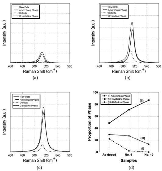
Lee, “Effective Ag Doping by He-Ne Laser Exposure to Improve the Electrical and the Optical Properties of CdTe Thin Films for Heterostructured Thin Film

Improvement of the Performance and Stability of Oxide Semiconductor Thin-Film Transistors Using Double-Stacked Active Layers.. Metal oxide semiconductor