I. INTRODUCTION
According to the development of MVL theory, the
need for MVL circuit design is increased. Two kinds of MVL circuit generally used, voltage-mode and current-mode. Current-mode MVL circuits have power consumption serious problem. Conversely, voltage-mod MVL circuits have the advantage of low power consumption. But since they require the multi-level ion implantation process technology to realize multi-threshold voltages in MOS transistors, complex fabrication and high cost are inevitable[1].
* 인하대학교 전자공학과
(Dept. of Electronic Eng., InHa Univ.)
接受日:2003年 7月 21日, 修正完了日:2004年 6月 25日
Pass-transistor Logic with neuron MOS Threshold gate
뉴런 MOS 임계 게이트를 갖는 2중 패스-트랜지스터 논리를 이용한 4치 논리 게이트 설계
박 수 진*, 윤 병 희*, 김 흥 수*
Soo - Jin Park*, Byoung-Hee Yoon*, Heung-Soo Kim*
Abstract
A multi-valued logic(MVL) pass gate is an important element to configure multi-valued logic. In this paper, we designed the Quaternary MIN(QMIN)/negated MIN(QNMIN) gate, the Quaternary MAX(QMAX)/negated MAX(QNMAX) gate using double pass-transistor logic(DPL) with neuron MOS(ν MOS) threshold gate. DPL is improved the gate speed without increasing the input capacitance. It has a symmetrical arrangement and double-transmission characteristics. The threshold gates composed by νMOS down literal circuit(DLC). The proposed gates get the valued to realize various multi threshold voltages. In this paper, these circuits are used 3V power supply voltage and parameter of 0.35um N-Well 2-poly 4-metal CMOS technology, and also represented HSPICE simulation results.
요 약
다치 논리 패스 게이트는 다치 논리를 구성하기 위한 중요한 소자이다. 본 논문에서는, 뉴런 MOS(νMOS) 임 계 게이트를 갖는 2중 패스-트랜지스터 논리를 이용하여 4치 MIN(QMIN)/negated MIN(QNMIN) 게이트 그리고 4 치 MAX(QMAX)/negated MAX(QNMAX) 게이트를 설계하였다. DPL은 입력 캐패시턴스의 증가 없이 게이트 속도 를 향상 시켰다. 또한 대칭 배열과 2중 전송 특성을 갖는다. 임계 게이트는 νMOS 다운 리터럴 회로(DLC)로 구성 된다. 제안된 게이트는 다양한 다치 임계 전압을 실현할 수 있다. 본 논문에서, 회로는 3V의 전원 전압을 사용하였 고 0.35um N-Well 2-poly 4-metal CMOS 공정의 파라메터를 사용하였으며 모든 모의 실험은 HSPICE를 이용하였 다.
Keyword : quaternary, DPL, QMIN/QNMIN, QMAX/QNMAX
In order to solve these problems, we try to use a general CMOS process to realize voltage-mode MVL circuits. A pass gate is a popular way to realize a MVL function. The algorithm for simplification of pass gate has already been developed[2][3].
A neuron-MOS(νMOS) is a kind of novel transistor device with multi-input gates[4]. The ν MOS is characterized by a variable threshold voltage achieved by controlling the voltages of the multi-input gates.
To voltage-mode MVL circuits, we present a ν MOS down literal circuit(DLC) in this paper. νMOS DLC is applied to MVL pass gate as the threshold gate, and the MVL pass gate can be fabricated with the common CMOS process[5].
Double pass-transistor logics(DPL)[6] gain their speed advantage over CMOS due to their high logic functionality. Also DPL has been developed to improve circuit performance at reduced supply voltage. A symmetrical arrangement and the double-transmission characteristics of the DPL gate compensate for the speed degradation due to the usage of both PMOS and NMOS pass transistors.
In this paper, we designed the quaternary logic gate using the DPL with νMOS threshold gate that has multi-threshold voltage. The νMOS threshold gate is designed using DLC. The quaternary logic gates include the quaternary MIN(QMIN)/negated MIN(QNMIN) and quaternary MAX(QMAX)/negated MAX(QNMAX). These proposed gates are confirmed by HSPICE simulations with 0.35um 2-poly 4-metal CMOS technology and 3V power supply voltage.
The MOS MVL circuits can be realized without the multi-level ion implantation process technology. The ease of fabrication will make MVL circuits more practically.
II. QUATERNARY LOGIC GATES
2.1. νMOS
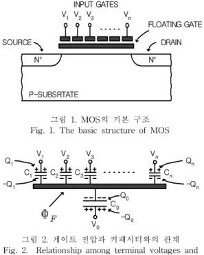
The basic structure of the functional νMOS transistor is shown in Fig.1. It is an n-channel ν MOS transistor having a gate electrode which is electrically floating. The multi-input gates are capacitively coupled to the floating gate. The terminal voltages and various capacitive coupling coefficients are defined in Fig.2, where ΦF is the floating-gate potential, V1, V2,···,Vn are the input signal voltages, C1, C2,···,Cn the capacitive coupling coefficients between the floating gate and each of the input gates, C0 is the capacitive coupling coefficient between the floating gate and the
substrate, and Q1, Q2,·· ·,Qn are the stored charges in each of the capacitors. A symbol representing the device is given in Fig. 3.
DRAIN SOURCE
N+ N+
P-SUBSRTATE
INPUT GATES V1 V2 V3 Vn
FLOATING GATE
그림 1. MOS의 기본 구조 Fig. 1. The basic structure of MOS
V1 V2 V3 Vn
V0 C0
Q0
C1 C2 C3 Cn
-Q0 -Q1
Qn
-Qn Q1
그림 2. 게이트 전압과 커패시터와의 관계 Fig. 2. Relationship among terminal voltages and
capacitance coupling coefficients
V1 V2 V3 Vn
그림 3. νMOS 심볼 Fig. 3. The symbol of the νMOS 2.2. DLC
A DLC is the fundamental element in MVL circuits. MVL logic functions are almost always developed from the down literal function, and most MVL circuits consist of DLC. The down literal function is by Eq.(1).
+
≥
≤
= −
1 0
) 1
( x i
i x x R
Di
(1)
Where, i⊆{0,1,⋅ ⋅⋅,R−2},x⊆{0,1,⋅ ⋅⋅,R−1}.
The νMOS DLC consists of p-channel νMOS (Pν MOS) and n-channel νMOS (NνMOS) as shown Fig.4.
V d d
V b 1
V b 2
V i n V o u t
nνM O S pνM O S
그림 4. νMOS DLC의 회로 Fig.4. Circuit description of νMOS DLC The common input to PνMOS and NνMOS, Vin is taken as the input of the DLC, and Vb1, Vb2 are bias voltages. VTC shown in Eq.(2).
2
2
1 b
b DD
TC
V V V
V = − +
(2)
Here, the restriction of Vb1, Vb2 is derived from saturation condition of νMOS transistors in the circuit. VTC of this circuit can be varied by controlling the values of the bias voltages(Vb1, Vb2), and different down literal functions can be implemented.
2.3. Threshold gate
According to Eq.(2), the quaternary DLC can be designed. There are three kinds of down literal functions in the quaternary system. Di(x)(i=0,1,2) can be attained by setting Vb1 and Vb2 to the values stated in Table 1.
표 1. 바이어스 전압에 따른 VTC의 변화 Table 1. The transformation of VTC about Bias
voltage
The symbols of the threshold gates are show in Fig. 5 and also its transfer characteristic of the threshold gates.
05
(a)15
(b)25
(c)(d)
그림 5. (a)Vth=0.5 (b)Vth=1.5 (c)Vth=2.5 (d)전달 특성 곡선
Fig. 5. (a)Vth=0.5 (b)Vth=1.5 (c)Vth=2.5 (d)Transfer characteristic curve
The truth table of quaternary literals is listed in Table 2.
표 2. 4치 리터럴의 진리표
Table 2. The truth table of the quaternary literals
2.4. DPL
Suzuki et al.[6] proposed the DPL that overcomes all the problems of complementary pass-transistor logic(CPL), namely, when implementing CPL, particularly in reduced supply voltage designs, it is import to take into account the problems of noise margins and speed degradation.
DPL consist of both nMOS and pMOS pass
VDD=3.3V VTC Vb1 Vb2
Vth(0.5) 0.5V 3V 2V
Vth(1.5) 1.5V 2.2V 0.8V
Vth(1.5) 2.5V 1V 0V
X X0 X1 X2 X3 X01 X02 X12 X13 X23
0 3 0 0 0 3 3 0 0 0
1 0 3 0 0 3 3 3 3 0
2 0 0 3 0 0 3 3 3 3
3 0 0 0 3 0 0 0 3 3
transistors, in contrast to CPL. So DPL give improved circuit performance at reduced supply voltage.
The CPL consists only of nMOS transistors, resulting in low input capacitance and high-speed operation. However, the abovementioned problems are caused by the high output signal level being lower than the supply voltage Vcc by the nMOS threshold voltage Vth. The usual way to avoid this is to use CMOS pass-transistor logic. Full-swing operation is attained by simply adding pMOS transistor in parallel with the nMOS transistors. In the DPL, the inputs to the gates of the pMOS transistor are changed. This arrangement compensates for the speed degradation of CMOS pass-transistors. DPL are symmetrical whereby the load in any DPL is distributed equally among the inputs. This result in a balanced input capacitance and reduces the dependence of the delay time on data. Also DPL has double-transmission characteristics[6].
2.5. QMIN/QNMIN, QMAX/QNMAX
We proposed the QMIN/QNMIN circuit. The QMIN operation is shown as Eq.(3). The operator
․ or ︿ is QMIN operation.
) , 1, 2 (
1 x xn QMIN x xn
x • •⋅ ⋅⋅• = ⋅ ⋅⋅
) , 1, 2 (
1 x xn QMIN x xn
x ∧ ∧⋅ ⋅⋅∧ = ⋅ ⋅⋅ (3)
A QMIN function shown in Table 3 is represented to Eq.(4).
표 3. QMIN 진리표 Table 3.The truth table of QMIN
0
0 0 0 0
0 0
1 1
1 1
1 2
2
2 BA
3
3 0
0 1
1 2
2 3
According to Eq.(4), (5) QMIN and QNMIN can be easily configured using DPL with MOS threshold gate.
+ < >+ < >
>
<
+
>
<
=
3 02
23 13 01 0
, , 0
B A B A B
B A A B Y
(4)
+ < >+ < >
>
<
+
>
<
=
3 02
23 13 01 0
, , 3
B A B A B
B A A B Y
(5)
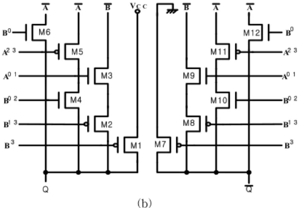
Where Fig.6(b), two input A and B are connected in the gate of pass transistor. MOS are turned on or turned off by the input value. Therefore, the output value is generated by QMIN/QNMIN operation.
(a)
Q Q
B0 A2 3
A0 1 B0 2 B1 3 B3
B0 A2 3 A0 1 B0 2 B1 3 B3 A
A
B A A B VC C
M1 M2 M3 M4 M5 M6
M7 M8
M9 M10 M11
M12
(b)
그림 6. (a)QMIN/QNMIN의 심볼 (b)QMIN/
QNMIN의 회로
Fig. 6. (a)Symbol of the QMIN/QNMIN. (b)A circuit of the QMIN/QNMIN.
For example, when input A is 2 and B is 3, M3, M9 are turned off and M5, M11 are turned on by input A, and M4, M10, M6, M12 turned off and M1, M7, M2, M8 turned on by input B, therefore, the output is "Q=2, Q=1"
Similarly, QMAX/QNMAX operation is shown as Eq.(6). The operator ∨ or ⊕ is QMAX operation.
1 2 ( 1, , ) ) , 1, 2 (
1
xn x n QMAX x x
x
xn x n QMAX x x
x
⋅
⋅
⋅
=
⊕
⋅
⋅
⋅
⊕
⊕
⋅
⋅
⋅
=
∨
⋅
⋅
⋅
∨
∨
(6)
A QMAX function shown in Table 4 is represented to Eq.(7).
표 4. QMAX의 진리표 Table 4. The truth table of QMAX
0
0 0 1 2
1 2
1 1
1 2
2 2
2
2 BA
3
3 3
3 3
3 3
3 3
According to Eq.(7), (8) QMAX and QNMAX can be easily configured using DPL with MOS threshold gate.
+ < >+ < >
>
<
+
>
<
=
0 13
01 02 23 3
, , 3
B A B A B
B A A B Y
(7)
+ < >+ < >
>
<
+
>
<
=
0 13
01 02 23 3
, , 0
B A B A B
B A A B Y
(8)
In Fig.7(b), the operation of QMAX/QNMAX same as the operation of the QMIN/QNMIN.
Also for example, when input A is 2 and B is 3, M3, M9 are turned off and M5, M11 are turned on by input A, and M4, M10, M6, M12 turned off and M1, M7, M2, M8 turned on by input B, therefore, the output is "Q=3, Q=0"
(a)
Q Q
B0 A2 3 A0 1 B0 2 B1 3 B3
B0 A2 3 A0 1 B0 2 B1 3 B3 A
A A B VC C B A
M1 M2 M3 M4 M5 M6
M7 M8 M9
M10 M11
M12
(b)
그림 7. (a)QMAX/QNMAX의 심볼 (b)QMAX/
QNMAX의 회로
Fig. 7. (a)Symbol of the QMAX/QNMAX. (b)A circuit of the QMAX/QNMAX
III. SIMULATION RESULTS
The HSPICE simulation of QMIN/QNMIN and QMAX/QNMAX are shown in Fig. 8(a) and (b), respectively.
The power dissipation, QMIN/QNMIN and QMAX/ QNMAX have 4.898uW. Each component is designed at the sampling speed of 0.25MHz.
(
a)
(b)
(c)
그림 8. 모의 실험 결과 (a) 입력 (b)QMIN/QNMIN (c)QMAX/QNMAX
Fig. 8. Simulation results (a) Input (b)The QMIN/QNMIN (c)The QMAX/QNMAX
IV. CONCLUSION
In this paper, we designed the quaternary logic gates such as QMIN/QNMIN and QMAX/QNMAX using double pass-transistor logic with neuron MOS threshold gate. The circuit verification of these logic circuits are verified by HSPICE simulation with CMOS 0.35um device parameter. Furthermore, we expect the implementation of quaternary full adder using the proposed the quaternary gates.
References
[1] T.Higuchi and M.Kameyama. "Multiple-Valued Digital Processing System," syokodo, Japan, 1989.
[2] O. Ishizuka, "Synthesis of a pass transistor
network applied to multi valued logic," Proc. 16th ISMVL, pp. 51-57. May 1986
[3] O.Ishizuka and J.Xu. "Simplification of pass transistor network and its applications," In proc. 17th ISMVL, pages 292-297,1987
[4] Tadashi Shibata, "A functional MOS transistor featuring gate-level weighted sum and threshold operations," IEEE Trans Electron device, vol.39, no.6, June.1992.
[5] Jing Shen, "Down literal circuit with neuron MOS transistor and its applications," Proc. 29th ISMVL, pp 180-185, May 1999
[6] Makato Suzuki et al., "A 1.5ns 32-b CMOS ALU in Double Pass-Transistor Logic," IEEE Journal of Solid State Circuits, Vol. 28., No. 11, Nov 1993.
[7] Jing Shen, "Multi-valued logic pass gate network using neuron-MOS transistors," IEEE, pp.180-185, May 1999.
[8] S. L. Hurst, "Multivalued logic-Its status and its future," IEEE Trnas. Comput., vol. C-33, pp.
1160-1179, 1984
[9] T. Shibata, "Neuron MOS binary-logic.
integrated circuits-part I: Design fundamentals and soft hardwarelogic circuit implementation." IEEE Trans Electron device, vol.40, no.3, pp.570-576, Mar.1993
[10] Rajesh S. Parthasarathy, "Double pass-transistor logic for high performance wave pipeline circuits," VLSI Design, Proc, 1998 Eleventh International conference on, 4-7, pp 495-500, Jan 1998.
[11] C. Smith, "The prospects for multivalued logic: A technology and applications view,"
IEEE Trans. Comput., vol. C-26, no.9, pp.619 634, Sept. 1981.
저 자 소 개
박 수 진 (朴 秀 珍, Soo-Jin Park) 제 8 권 제 1호 논문 03-02-03 참조 인하대학교 전자공학과 박사과정
윤 병 희 (尹 炳 熙, Byoung-Hee Yoon) 제 7 권 제 1호 논문 03-01-05 참조 인하대학교 전자공학과 박사수료 김 흥 수(金 興 壽, Heung-Soo Kim) 제7 권 1호 논문 03-01-05 참조 인하대학교 전자공학과 교수