S대역 군사 레이더용 2kW급 GaN HEMT 증폭기 개발
김시옥*ㆍ최길웅**ㆍ유영근***ㆍ임병옥****ㆍ김동길*****ㆍ김흥근******
Development of 2-kW Class C Amplifier Using GaN High Electron Mobility Transistors for S-band Military Radars
Si-Ok Kim*ㆍGil-Wong Choi**ㆍYoung-Geun Yoo***ㆍByeong-Ok Lim****ㆍ Dong-Gil Kim*****ㆍHeung-Geun Kim******
요 약
본 논문에서는 S-밴드 군용 레이더에 사용되고 기존의 TWTA를 대체하기 위해 GaN HEMT 기반 증폭모듈 을 이용하여 개발한 2kW급 반도체증폭기(SSPA)를 제안하였다. 제안한 SSPA는 8개의 증폭모듈로 이루어진 고 출력증폭모듈, 구동증폭모듈, 제어모듈 및 전원공급 장치로 이루어져 있다. 제안한 SSPA는 1) 증폭모듈과 구성 부품은 공간적 제약으로 작은 패키지에 통합설계 되었으며, 2) PCB 내장형 하모닉필터를 이용하여 고주파를 제 거하였으며, 그리고 3) 입력신호의 듀티 변화에 대응하여 일정한 출력이 유지되도록 하는 자동이득조절기를 설 계하였다. 제안된 SSPA는 최대 48 dB의 이득과 3.1~3.5 GHz의 주파수 대역에서 63-63.6 dBm의 출력 전력을 보였다. 자동이득조절 기능은 15-20 dBm의 입력전력 변동에도 대해서, 출력전력이 63dBm 전후로 일정하게 유 지하는 것을 확인하였다. 마지막으로 MIL-STD-810의 시험기준을 만족하는 높은 (55 ℃) / 낮은 (-40 ℃) 온도 시험 프로파일을 이용한 온도시험을 통해 개발된 시스템의 신뢰성을 검증하였다. 개발된 SSPA는 경량, 고출력, 고이득, 안전기능, 낮은 수리비, 짧은 수리시간 등 측면에서 기존의 TWTA 증폭기보다 우수한 것을 확인하였다.
ABSTRACT
This paper proposes a 2-kW solid-state power amplifier (SSPA) developed by employing power amplifier pallets designed using gallium-nitride high electron mobility transistors, which is used in S-band military radars and to replace existing traveling-wave tube amplifier (TWTA). The SSPA consists of a high-power amplifier module, which combines eight power amplifier pallets, a drive amplifier module, a digital control module, and a power supply unit.
First, the amplifier module and component were integrated into a small package to account for space limitations; next, an on-board harmonic filter was fabricated to reject spurious components; and finally, an auto gain control system was designed for various duty ratios because recent military radar systems are all active phase radars using the pulse operation mode. The developed SSPA exhibited a max gain of 48 dB and an output power ranging between 63-63.6 dBm at a frequency band of 3.1 to 3.5 GHz. The auto gain control function showed that the output power is regulated around 63 dBm despite the fluctuation of the input power from 15-20 dBm. Finally, reliability of the developed system was verified through a temperature environment test for nine hours at high (55 ℃) / low (-40℃) temperature profile in accordance with military standard 810. The developed SSPA show better performance such as light weight, high output, high gain, various safety function, low repair cost and short repair time than existing TWTA.
키워드
GaN HEMT, S-band, Solid State Power Amplifier, Transmitter GaN HEMT, S대역, 반도체 전력 증폭기, 송신기
* 경북대학교 전기공학과 / 국방기술품질원 선임연구원([email protected])
** 한화시스템 수석연구원([email protected])
*** 브로던 연구이사([email protected])
ㆍ접 수 일 : 2020. 04. 07 ㆍ수정완료일 : 2020. 05. 11 ㆍ게재확정일 : 2020. 06. 15
ㆍReceived : Apr. 07, 2020, Revised : May. 11, 2020, Accepted : Jun. 15, 2020 http://dx.doi.org/10.13067/JKIECS.2020.15.3.421
Ⅰ. Introduction
High efficiency power amplifiers (PAs) are one of the most important components in modern radar systems, used to transmit a powerful RF signal for object detection and tracking. In past decades, vacuum-tube electronics such as the traveling wave tube amplifier (TWTA) have been used in high power amplifiers, particularly in military radar applications. However, TWTAs have several drawbacks such as a short life-time, requirement of warm-up time, and power degradation issues [1, 2].
Recently, solid-state power amplifier (SSPA) based on a Si BJT and GaAS high electron mobility transistors (HEMTs) have been reported to have an impressive power output, higher than several hundreds of watts, in the L to C frequency band [3-9]. However, most studies are limited to several hundreds of watts. It is hard to search previous study which related to the several kilowatts amplifiers design and implement, especially military radar system [2, 10-11].
However, these SSPA must be constructed using a number of modules to obtain a power level of several kilowatts. A large number of power modules increases the complexity of a control system, and the DC power distribution and RF signal combination require a large physical space.
With advancement in the device technology of GaN HEMTs, which has led to the realization of high breakdown field, high electron density, and high electron saturation velocities compared to those of Si and GaAs, the SSPA using GaN HEMTs can be made more compact and subsequently, be used to replace the TWTAs in military radar systems.
However, some challenges still need to be overcome to realize a power amplifier with a capacity of several kilowatts for military radar systems; these include i) the integration of a small sized harmonic filter to reject spurious components
caused by the multi-stage combiner, ii) the development of an auto control system in order to supply constant input power into high power amplifier in spite of variable duty ratios because all recent military radar systems are active phase radar using the pulse operation mode, and iii) the high reliability under extreme environment conditions such as under high (55 ℃ above) / low (-40 ℃ below) temperatures to satisfy military standard.
In this study, a 2-kW GaN HEMT-based S-band SSPA for military radars, which consists of a high power amplifier (HPA) module, drive amplifier (DA) module, control module, and power supply unit, was designed and implemented in order to not only replace existing TWTAs but also reduce cost and improve maintainability. The SSPA also incorporated on-board harmonic filter, auto gain control function and satisfy military level reliability requirement such as MIL-STD-810[12]. To realize the HPA module, the multi-stage combination configuration involving eight GaN HEMT-based PA pallets was used. The performance of the developed SSPA was measured in the pulse operation mode with several duties. Its reliability was verified through a temperature environment test to ensure satisfactory operation under extreme temperature conditions for military radar system.
Ⅱ. Proposed Solid State Power Amplifier Design
2.1 Design of High Power Amplifier Module The HPA module was designed to operate in the pulse mode with a width of 22 μs and a maximum duty cycle of 15.5%. To derive the total output power of 63 dBm from the input power of 15 dBm, the HPA must have a power gain of 48 dB in the S-band. The pulse droop is maintained to be less than 0.5 dB for flattening the output power. The designed HPA possesses some functionalities for
Connector DRA1 Connector Thermopad Divider Attenuator DRA2 Attenuator HPA*8 Combiner Connector TOTAL
Gain(dB) 0 11.34 -0.5 -6 -9.5 -5 24.5 -5 33 8.1 -0.3 47.57
Power(dBm) 15 26 25.5 19.5 10 5 27 22 54.77 62.87 62.57 62.57
OP1dB(dBm) 26 27 54.77
HPA DRA
그림 2. SSPA 이득 분배도 Fig. 2 Gain budget for overall SSPA
Har mo nic Filte r Fixed Attenuator Drive
Amplifier PA Pallet (Class C Amp)
AGC Module
RF IN
Control Module Processer
REF. REF.
RF OUT Variable
Attenuator
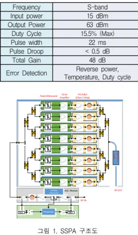
그림 1. SSPA 구조도
Fig. 1 Block diagram of the proposed SSPA
Frequency S-band
Input power 15 dBm
Output Power 63 dBm
Duty Cycle 15.5% (Max)
Pulse width 22 ms
Pulse Droop < 0.5 dB
Total Gain 48 dB
Error Detection Reverse power, Temperature, Duty cycle 표1. 고출력증폭기 모듈의 사양서 Table 1. Specification of the high power amplifier
(HPA) module error detection, such as the presence of i) excess
reverse power in the case of mismatching of cable interconnection, ii) high temperature alarm in the HPA module, and iii) different duty cycle of the input control signal. The specifications of the HPA are listed in Table 1.
In particular, the S-band HPA module was designed to achieve the overall output power and gain, a high efficiency, and effective thermal radiation for environment reliability. It consists of input dividers, output combiners, eight drive amplifiers, and eight PA pallets. The input dividers and output combiners were manufactured by Low Temperature Cofired Ceramic (LTCC) technology for high power applications. And thanks to high density property of LTCC technology, it is possible that HPA module can be manufactured with small size cabinet. Between the PA pallets and the input divider, the fixed attenuators and the drive amplifiers was used for stabilizing and driving the input power level. The PA pallets combined with the 8-way configuration are used to achieve the desired output power and total gain. A hybrid branch-line coupler (HBC) is designed in the first and second combiners, and a T-junction combiner is adopted in the final combiner owing to its high power capability. Figures 1 and 2 show the block diagram of the high power module and present the power budget, respectively.
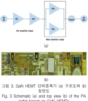
2.2 Design of Power Amplifier Pallet
(a)
(b)
그림 3. GaN HEMT 단위증폭기 (a) 구조도와 (b) 정면도
Fig. 3 Schematic (a) and top view (b) of the PA pallet based on GaN HEMTs
표 2. 전력 증폭기(PA) 팔레트 사양 Table 2. Specifications of power amplifier (PA)
pallet
Frequency S-band
Input power 24 dBm Output Power 55 dBm Pulse width 200 ms Pulse Droop < 0.3 dB
Total Gain 31 dB
그림 4. PCB 내장 하모닉필터 Fig. 4 Image of Harmonic filter on the PCB
그림 5. 자동이득조절기의 상세 구조도 Fig. 5 Detail block diagram of auto level control
module The PA pallet consists of a pre-amplifier stage,
main amplifier stage, and isolator, as shown in Figure 3. Two GaN-based HEMTs inter-connected in the parallel balanced configuration are used to obtain high output power and improve the reliability characteristics in the main amplifier stage. GaN-based HEMTs are used in the PA module. Compared to other material devices, the GaN-based HEMTs demonstrate excellent performance in the form of high power, high efficiency, and high gain. The pre-amplifier stage was used in a cascade configuration to ensure low input power. The isolator was used to increase the isolation level to protect the power amplifier pallet.
In the pulse operation mode, with a width of 200 μ s and the input power of 24 dBm, the fabricated PA pallet exhibited an output power of 55 dBm, power gain of 31 dB, and drain efficiency of 40%.
The measured gain flatness and pulse droop were 0.7 and 0.3 dB, respectively. The specifications of a pallet are summarized in Table 2.
2.3 Harmonic Filter and Auto Gain Control Apart from the aforementioned challenges to realize a several kilowatts power amplifier, TWTAs radar systems involve other issues. The TWTAs includes an external harmonic filter to reject spurious signals, which is large size, heavy weight and hard to maintain; this is because no systems can be incorporated internally in TWTAs. To overcome this issue, a harmonic filter is designed on the PCB which owing to the existence of the SSPA structure as shown in Figure 4. As a result, the proposed amplifier system may lead to not only low maintenance cost but also size and weight reduction.
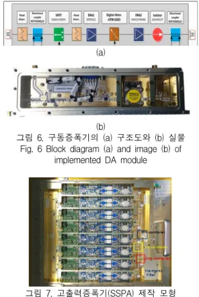
(a)
(b)
그림 6. 구동증폭기의 (a) 구조도와 (b) 실물 Fig. 6 Block diagram (a) and image (b) of
implemented DA module
그림 7. 고출력증폭기(SSPA) 제작 모형 Fig. 7 Image of implemented high power amplifier
module Recent military radar systems are active phase
array radars and are operated in the pulse operation mode, in which the duty ratio of the power signal changes dynamically. Consequently, the average input signal power supplied to the HPA module also changes. However, the HPA module requires a specific level of input signal power in order to operate properly. In the case considered in this study, the input signal power to the HPA module should be larger than 23 dBm to satisfy the amplifier operation condition.
To provide a constant input signal power for the HPA module, an auto gain control (AGC) module is implemented in initial stage of SSPA (Figure 5).
The ALC module measures both the input signal power and output signal power, and then adjusts the digital attenuator level automatically to ensure constant signal power.
2.4 Thermal Radiation Structure Design The SSPA is developed particularly for military radar systems. Therefore, it is necessary that the SSPA is capable of operating under extreme environment conditions such as extreme high or low temperatures condition. To ensure environment reliability, designed SSPA have to satisfy the MIL-STD-810 environment test requirement. In order that, structure and external case which considering thermal dissipation design was made.
To verify thermal radiation structure, thermal radiation simulation using ANSYS is conducted.
And temperature test according MIL-STD-810 temperature test procedure is executed.
Ⅲ. Implementation and Measurement Results
3.1 Drive Amplifier Implementation
Figure 6 shows the block diagram of the DA modules and an image of the implemented DA
modules. BT05VG2 and HMC327MS8GE chips are used for the pre-amplifier, and AT90-0283 is adopted as the digital attenuator for auto gain control module which attenuate input signal in 0.5 dB steps to 15.5 dB.
3.2 High Power Amplifier Module Implementation
To realize a 2-kW amplifier, PA pallets in an 8-way configuration are used to achieve the desired output power and total gain. The first and second combiners are designed using a hybrid branch-line coupler with RCP3500A03 LTCC coupler. The final combiner is implemented with T-junction technology to support high power capability. Figure 7 shows the 2-kW 8-way HPA module with an on-board harmonic filter.
3.3 Measurement Results
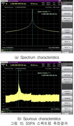
3.3.1 Amplifier Performance Measurement The performance of the developed SSPA was measured in the pulse operation with a width of 22 μs, duty of 10-15%, and input power of 15 dBm.
Figure 8 depict power measurement system configuration. Figure 9 shows the rising and falling times of the output power. The measurement times were 14.6 and 16.5 ns for 10% duty, and 14.6 and 23.2 ns for 15% duty, respectively. The SSPA demonstrated an output power of 63 dBm and a power gain of 48 dB. From the spectrum analysis shown in Figure 10, the output power and spurious level were measured to be 63 dBm and less than -40 dBc, respectively.
The output power measurement results with various frequencies and two duty ratio are shown in Figure 11. The output power is higher than 63 dBm for the given frequency ranges and duty ratio.
The total power efficiency for 5 frequency points with duty 15% is summarized in Table 3. As shown in Table 3, the maximum efficiency is 32%.
The proposed the proposed SSPA module exhibits high gain, good output power and better efficiency when it is compared with similar power amplifier for S-band radar in which total efficiency is 26.2%
[13]. Finally, the ALC function was evaluated by measuring the output power with respect to different input power signals, various frequencies, and two duty ratio, and the results are shown in Figure 12. The output power was regulated around 63 dBm despite the change in input power from 15-20 dBm.
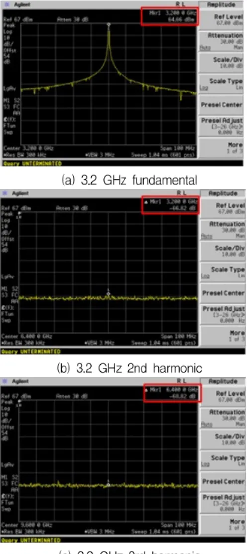
3.3.2 Harmonic Filter Performance Measurement
The performance of on-board harmonic filter was measured for 3.2 GHz signal. Figure 13 depict measurement result for 3.2 GHz fundamental and harmonic components signal. As shown in Figure
13(b) and 13(c), harmonic components are well suppressed in which harmonic signal power is lower than -66 dB. And Figure 14 shows a harmonic filter characteristic.
3.3.3 Temperature Reliability Test
Owing to the high thermal radiation of the HPA, the SSPA was designed to have a thermal dissipation structure: Cooling air with 70.62 CFM flows into the base plate, as shown in Figure 15(a).
Using the commercial simulator, ANSYS ICEPAK, the thermal effect was simulated. From the simulated results in Figure 15(b), the maximum temperature of the SSPA is estimated to be 88.4 C, which represents a safe value in the pulse mode operating condition of the military radar system.
To ensure temperature reliability, a temperature environment test was conducted according MIL-STD-810 procedure for extreme temperature conditions 1) high temperature, ~55 ℃, 2) low temperature, approximately -40℃. Figure 16 shows the temperature change profile for a testing period of nine hours. Figure 17 shows the SSPA output power results during the temperature environment test. Table 4 presents the difference in the output power of the SSPA between different temperature conditions for five major frequency points in the S-band. The average of the difference of the output power is less than 0.1 dB. The device thus operates well under extreme temperature environment condition, and also supplies nearly constant output power regardless of the temperature changes.
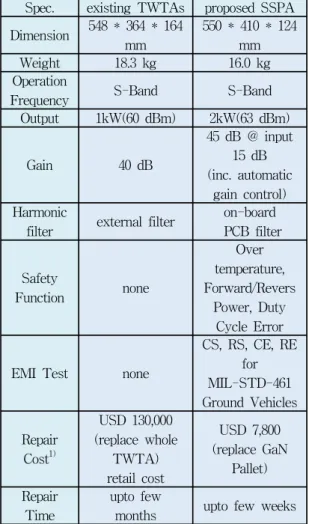
Finally, the superior points of designed SSPA are summarized compared to the specifications of the existing TWTA including dimension, weight, repair cost/time, etc. in Table 5. The proposed SSPA show better performance such as light weight, high output, high gain, various safety function, low repair cost and short repair time than existing TWTA
그림 8. 성능측정을 위한 시험환경 구성도 Fig. 8 Output power measurement system
configuration
(a) Duty: 10%
(b) Duty: 15%
그림 9. SSPA 상승/하강시간 측정결과 Fig. 9 Rising/falling times and output power of
the SSPA with different duty ratios
.
(a) Spectrum characteristics
(b) Spurious characteristics 그림 10. SSPA 스펙트럼 측정결과 Fig. 10 Spectrum and spurious characteristics of
the SSPA with 15% duty
그림 11. 주파수별 SSPA 출력측정결과 Fig. 11 Output power of the SSPA with various
frequencies
(a) Duty 10%
(b) Duty 15%
그림 12. 자동이득조절기의 성능측정 결과 Fig. 12 Performance of ALC with different duty
(a) 3.2 GHz fundamental
(b) 3.2 GHz 2nd harmonic
(c) 3.2 GHz 3rd harmonic
그림 13. 3.2 GHz 대역 하모닉필터 성능측정결과 Fig. 13 Harmonic filter characteristics of the SSPA for 3.2 GHz fundamental and harmonics
signal
그림 14. 하모닉필터 성능측정 결과 Fig. 14 Measurement result for harmonic filter
characteristics
(a) Top view
(b) Thermal distribution 그림 15. SSPA 열해석 시뮬레이션 결과 Fig. 15 Top view of the amplifier (a) and
thermal distribution (b) of the SSPA
Condition 3.1 GHz
3.2 GHz
3.3 GHz
3.4 GHz
3.5 GHz Normal vs.
Low 0.033 0.005 0.091 0.098 0.118 Normal vs.
High 0.132 0.076 0.048 0.002 0.043 Low vs.
High 0.099 0.081 0.139 0.096 0.075 Average 0.088 0.054 0.092 0.065 0.078
Spec. existing TWTAs proposed SSPA Dimension 548 * 364 * 164
mm
550 * 410 * 124 mm
Weight 18.3 kg 16.0 kg
Operation
Frequency S-Band S-Band
Output 1kW(60 dBm) 2kW(63 dBm)
Gain 40 dB
45 dB @ input 15 dB (inc. automatic
gain control) Harmonic
filter external filter on-board PCB filter
Safety
Function none
Over temperature, Forward/Revers
Power, Duty Cycle Error
EMI Test none
CS, RS, CE, RE for MIL-STD-461 Ground Vehicles Repair
Cost1)
USD 130,000 (replace whole
TWTA) retail cost
USD 7,800 (replace GaN
Pallet) Repair
Time
upto few
months upto few weeks 그림 16. MIL-STD-810 시험규격의 온도시험 조건
Fig. 16 Temperature control profile for temperature environment test with MIL-STD-810
그림 17. 온도시험 중의 SSPA 출력 측정 결과 Fig. 17 Output power of the SSPA during
temperature environment test
표 3. 5개 주파수대역에 대한 SSPA 증폭률 Table 3. Total efficiency of proposed 2kW SSPA
module for 5 frequency points with duty 15%
Frequency (GHz)
Output power (dBm)
Power consumption
(W)
Efficiency (%)
3.1 62.60 980 29%
3.2 62.93 942 32%
3.3 62.74 955 30%
3.4 62.09 1020 24%
3.5 61.99 985 25%
표 4. 온도조건에 따른 SSPA 출력전력 비교(크기) Table 4. Difference in output power of SSPA for different temperature conditions (only magnitude); unit: dB
표 5. 제안한 SSPA와 사용중인 TWTAs 비교 Table 5. Specification comparison between proposed
SSPA and existing TWTAs
1) Repair cost calculated using repair history and
Ⅳ. Conclusions
In this study, a 2-kW GaN HEMTs S-band SSPA for military radars system was designed and implemented including a harmonic filter, auto gain control function and high reliability for temperature.
The high power amplifier module consists of eight power amplifier pallets and a three-stage power combiner. The performance of the developed SSPA was measured in the pulse operation mode with two different duty ratio. The developed SSPA exhibited a maximum gain of 48 dB and an output power ranging between 63 to 63.6 dBm for a frequency band of 3.1 to 3.5 GHz. An auto gain control function was incorporated, through which the output power was regulated around 63 dBm despite fluctuations in the input power from 15-20 dBm. And Its environment reliability was verified through a temperature environment test according to MIL-STD-810 procedure including a high (55
℃) / low (-40 ℃) temperature test. The developed SSPA give better performance than existing TWTA with respect to various specification including weight, output power, gain and etc.
However, SSPA still have a problems of a designing a low insertion loss coupling system and a heating system due to a small unit output of a semiconductor based transmitter.
The proposed SSPA consists of several modules including DA module, HPA module, and miscellaneous modules. However, this paper focuses on the DA and HPA module, and the other modules are only briefly discussed. The power supply module is a commercial product operating on three-phase 200 V supply from the main power source of the radar system, and it supplies DC 48 V to the DA and HPA modules. The digital control module monitors the SSPA system conditions such as voltage, current, and temperature, and controls the operation of the amplifier modules.
References
[1] M. Hanczor and M. Kumar, “12 kW S-band Solid State Transmitter for Modern Radar Systems,”
IEEE Transactions on Microwave Theory and Techniques, vol. 12, 1993, pp. 2237-2242.
[2] K, Kim, Y. Lee, J. Joo, H. Kim, J. Choi, and D.
Park, “1.5 kW, S-Band Solid-State Pulsed Power Amplifier with digitally controlled Automatic Gain control Circuit,” Int. Conf. on Asia-Pacific Microwave Conference, Yokohama, Japan, Dec.
2006, pp. 714-717.
[3] H. Shigematsu, Y. Inoue, A. Akasegawa, M.
Yamada, S. Masuda, K. Kamada, A. Yamada, M.
Kanamura, T. Ohki, K. Makiyama, N. Okamoto, K. Imanishi, T. Kikkawa, K. Joshin, and N.
Hara, “C-band 340-W and X-band 100-W GaN power amplifiers with over 50-% PAE,” Int.
Conf. on IEEE MTT-S Int. Microwave Symp.
Digest, Boston, USA, June 2009, pp. 1265-1268.
[4] S. Yang, “Design and fabrication of SSPA module in X-band for Radar,” J. of the Korea Institute of Electronic Communication Science, vol. 13, no. 5, 2018, pp. 943-948.
[5] H. Maehara, H. Uchida H, N. Kosaka, E.
Kuwata, K. Yamanaka, J. Nishihara, K.
Kawashima, and M. Nakayama, “Internally matched GaN FET at C-band with 220 W output power and 56% power added efficiency,”
Int. Conf. on Asia-Pacific Microwave Conference, Kaohsiung, Taiwan, Dec. 2012, pp. 358-360.
[6] Y. Okamoto, T. Nakayama, Y. Ando, A.
Wakejima, K. Matsunaga, K. Ota, and H.
Miyamoto, “230 W C-band GaN-FET power amplifie,” Electronics Letter, vol. 43, no. 17, 2007, pp. 927-929.
[7] K. Krishnamurthy, M. Poulton, J. Martin, R.
Vetury, J. Brown, and J. Shealy, “A 250 W S-Band GaN HEMT amplifier,” Int. Conf. on IEEE Compound Semiconductor Integrated Circuit Symp., Portland, USA, Oct. 2007, pp. 1-4.
[8] H. Song, J. Kim, H. Kang, J. Song, C. Park, K.
Rhee, C. Lee, and D. Kim, “Development of SSPA-based X-band Transmitter with Graceful Degradation,” J. of the Korea Institute of Electronic Communication Science, vol. 14, no. 5, 2019, pp.
853-862.
[9] Z. Cheng, D. Zhu, G. Yan, G. Liu, and S. Gao,
“A 3-7 GHz GaN HEMT power amplifier,”
Microw. Opt. Technol. Lett. vol. 58, no. 4, 2016, pp. 901-904.
[10] J. Kwack, K. Kim, and S. Cho, “1 kW S-band solid state radar amplifier,” Int. Conf. on IEEE 12th Annual Wireless and Microwave Technology Conference, Florida, USA, Apr. 2012, pp. 1-4.
[11] S. Mohadeskasaei, F. Lin, X. Zhou, and S.
Abdullahi, “Design of a 2.5-kW L-band solid-state pulsed power amplifier for radar applications,” Electronics Letters, vol. 53, no. 15, 2017, pp. 1071-1073.
[12] Department of Defense(DoD), “Environmental Engineering Considerations and Laboratory Tests,” MIL-STD-810G w/Change-1, 2014. 4.
[13] J. Joo, G. Choi, S. Jang, J. Choi, and D. Park,
“1.5 kW solid-state pulsed microwave power amplifier for S-band radar application,” Int. Conf.
on 2006 IEEE Radio and Wireless Symposium, San Diego, USA, Oct. 2006, pp. 171-174.
저자 소개
김시옥(Si-Ok Kim) 2006년 경북대학교 전자전기컴퓨터 학부 졸업(공학사)
2014년 경북대학교 산업대학원 산 업공학과 졸업(공학석사)
2016년 ~ 경북대학교 전기공학과 (박사과정) 2012년 ∼ 현재 국방기술품질원 선임연구원
※ 관심분야 : RF power Amplifier, GaN Transistor, S patial Combiner, Radar & TRM
최길웅(Gil-Wong Choi) 2004년 광운대학교 전자공학부 졸 업(공학사)
2006년 광운대학교 대학원 전파공 학과 졸업(공학석사)
2011년 광운대학교 대학원 전파공학과 졸업(공학박사) 2011년 ∼ 현재 한화시스템 수석연구원
※ 관심분야 : RF power Amplifier, TRM 등
유영근(Young-Geun Yoo) 1994년 울산대학교 전자 및 전산기 공학과 졸업(공학사)
1996년 울산대학교 대학원 전자공 학과 졸업(공학석사)
2008년 울산대학교 대학원 전자공학과 졸업(공학박사) 1996년 ∼1999년 현대전자 위성사업단 연구원 1999년 ∼2007년 ㈜코모텍 책임연구원 2007년 ∼현재 ㈜브로던 연구이사
※ 관심분야 : SSPA Module, Microwave TRM
임병옥(Byeong-Ok Lim) 2000년 국립한경대학교 전자공학과 졸업(공학사)
2002년 동국대학교 대학원 전자공 학과 졸업(공학석사)
2009년 동국대학교 대학원 전자공학과 졸업(공학박사) 2017년 한화시스템 전문연구원
2018년 ∼현재 주)디에스전자 대표
※ 관심분야 : 레이다시스템, RF 고출력증폭기
김동길(Dong-Gil Kim) 2006년 경북대학교 전자전기컴퓨터 학부 졸업(공학사)
2008년 경북대학교 대학원 전자학 과 졸업(공학석사)
2015년 경북대학교 대학원 전자공학과 졸업(공학박사) 2015년 ∼ 2016년 국방기술품질원 선임연구원 2017년 ~ 현재 경일대학교 로봇공학과 조교수
※ 관심분야 : 무선통신시스템, 고장진단, 고장대처 제어
김흥근(Heung-Geun Kim) 1980년 서울대학교 공과대학 전기 공학과 졸업(공학사)
1982년 서울대학교 대학원 전기공 학과 졸업(공학석사)
1988년 서울대학교 대학원 전기공학과 졸업(공학박 사)
현재 경북대학교 전기공학과 교수 2015년 ∼현재 전력전자학회 명예회장
※ 관심분야 : 교류전동기 제어, 태양광 발전 및 마 이크로그리드 시스템